ZHCSC55A January 2014 – March 2014 UCD9244-EP
PRODUCTION DATA.
- 1 特性
- 2 应用范围
- 3 说明
- 4 修订历史记录
- 5 说明(继续)
- 6 Terminal Configuration and Functions
-
7 Specifications
- 7.1 Absolute Maximum Ratings
- 7.2 Handling Ratings
- 7.3 Recommended Operating Conditions
- 7.4 Thermal Information
- 7.5 Electrical Characteristics
- 7.6 Electrical Characteristics (Continued)
- 7.7 ADC Monitoring Intervals And Response Times
- 7.8 Hardware Fault Detection Latency
- 7.9 PMBus/SMBus/I2C
- 7.10 I2C/SMBus/PMBus Timing Requirements
- 7.11 Typical Characteristics
-
8 Detailed Description
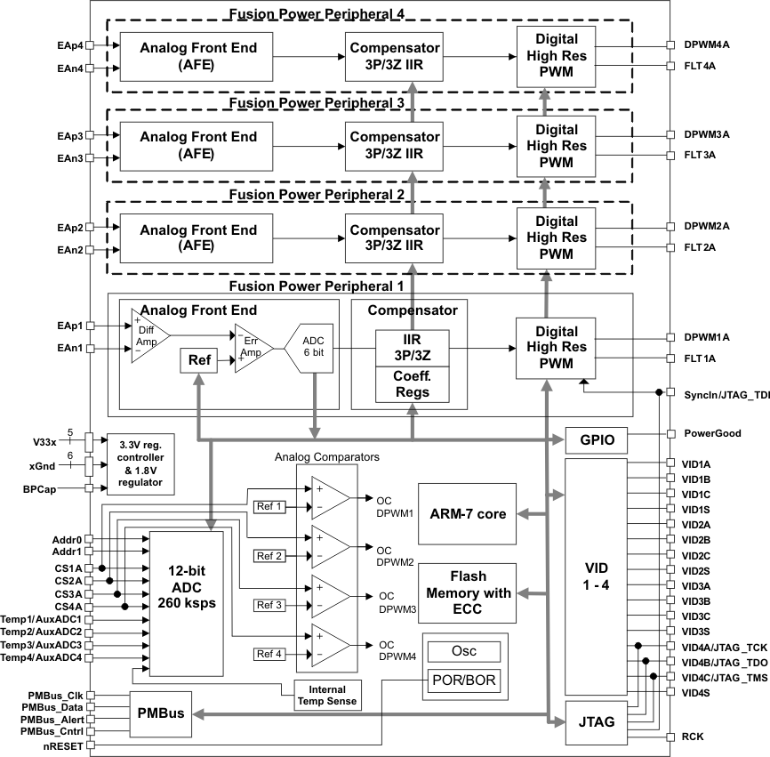
- 8.1 Overview
- 8.2 Functional Block Diagram
- 8.3
Feature Description
- 8.3.1 PMBus Interface
- 8.3.2 Resistor Programmed PMBus Address Decode
- 8.3.3 VID Interface
- 8.3.4 Jtag Interface
- 8.3.5 Bias Supply Generator (Shunt Regulator Controller)
- 8.3.6 Power-On Reset
- 8.3.7 External Reset
- 8.3.8 ON_OFF_CONFIG
- 8.3.9 Output Voltage Adjustment
- 8.3.10 Calibration
- 8.3.11 Analog Front End (AFE)
- 8.3.12 Voltage Sense Filtering
- 8.3.13 DPWM Engine
- 8.3.14 Rail/Power Stage Configuration
- 8.3.15 DPWM Phase Synchronization
- 8.3.16 Output Current Measurement
- 8.3.17 Current Sense Input Filtering
- 8.3.18 Over-Current Detection
- 8.3.19 Input Voltage Monitoring
- 8.3.20 Input UV Lockout
- 8.3.21 Temperature Monitoring
- 8.3.22 Auxiliary ADC Input Monitoring
- 8.3.23 Soft Start, Soft Stop Ramp Sequence
- 8.3.24 Non-Volatile Memory Error Correction Coding
- 8.3.25 Data Logging
- 8.4 Device Functional Modes
- 9 Applications and Implementation
- 10Power Supply Recommendations
- 11Layout
- 12Device and Documentation Support
- 13Mechanical, Packaging, and Orderable Information
8 Detailed Description
8.1 Overview
The UCD9244 contains four Fusion Power Peripherals (FPP). Each FPP consists of:
- A differential input error voltage amplifier.
- A 10-bit DAC used to set the output regulation reference voltage.
- A fast ADC with programmable input gain to digitally measure the error voltage.
- A dedicated 3-pole/3-zero digital filter to compensate the error voltage
- A digital PWM (DPWM) engine that generates the PWM pulse width based on the compensator output.
Each controller is configurable through the PMBus serial interface.
8.2 Functional Block Diagram
8.3 Feature Description
8.3.1 PMBus Interface
The PMBus is a serial interface specifically designed to support power management. It is based on the SMBus interface that is built on the I2C physical specification. The UCD9244 supports revision 1.2 of the PMBus standard. Wherever possible, standard PMBus commands are used to support the function of the device. For unique features of the UCD9244, MFR_SPECIFIC commands are defined to configure or activate those features. These commands are defined in the UCD92xx PMBUS Command Reference.
The UCD9244 is PMBus compliant, in accordance with the "Compliance" section of the PMBus specification. The firmware is also compliant with the SMBus 2.0 specification, including support for the SMBus ALERT function. The hardware can support 100 kHz, 400 kHz, or 1 MHz PMBus operation.
8.3.2 Resistor Programmed PMBus Address Decode
The PMBus Address is selected using resistors attached to the ADDR0 and ADDR1 terminals. At power-up, the device applies a bias current to each address detect terminal. The measured voltage on each terminal determines the PMBus address as defined in Table 1. For example, a 133kΩ resistor on ADDR1 and a 75kΩ on ADDR0 will select PMBus address = 100. Resistors are chosen from the standard EIA-E96 series, and should have accuracy of 1% or better.
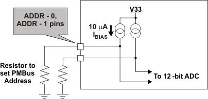 Figure 4. PMBus Address Detection Method
A short or open on either address terminal causes the PMBus address to default to address 126. To avoid potential conflicts between multiple devices, it is best to avoid using address 126.
Some addresses should be avoided; see Table 1 for details.
Table 1. PMBus Address Bins(1)
| ADDR0 | |||||||||||||||
| (short) < 36.5k |
42.2k | 48.7k | 56.2k | 64.9k | 75k | 86.6k | 100k | 115k | 133k | 154k | 178k | 205k | (open) > 237k |
||
 |
< 36.5k (short) |
126 | 126 | 126 | 126 | 126 | 126 | 126 | 126 | 126 | 126 | 126 | 126 | 126 | 126 |
| 42.2k | 126 | 126(2) | 1 | 2 | 3 | 4 | 5 | 6 | 7 | 8 | 9 | 10 | 11(3) | 126 | |
| 48.7k | 126 | 126(2) | 13 | 14 | 15 | 16 | 17 | 18 | 19 | 20 | 21 | 22 | 33 | 126 | |
| 56.2k | 126 | 24 | 25 | 26 | 27 | 28 | 29 | 30 | 31 | 32 | 33 | 34 | 35 | 126 | |
| 64.9k | 126 | 36 | 37 | 38 | 39 | 40 | 41 | 42 | 43 | 44 | 45 | 46 | 47 | 126 | |
| 75k | 126 | 48 | 49 | 50 | 51 | 52 | 53 | 54 | 55 | 56 | 57 | 58 | 59 | 126 | |
| 86.6k | 126 | 60 | 61 | 62 | 63 | 64 | 65 | 66 | 67 | 68 | 69 | 70 | 71 | 126 | |
| 100k | 126 | 72 | 73 | 74 | 75 | 76 | 77 | 78 | 79 | 80 | 81 | 82 | 83 | 126 | |
| 115k | 126 | 84 | 85 | 86 | 87 | 88 | 89 | 90 | 91 | 92 | 93 | 94 | 95 | 126 | |
| 133k | 126 | 96 | 97 | 98 | 99 | 100 | 101 | 102 | 103 | 104 | 105 | 106 | 107 | 126 | |
| 154k | 126 | 108 | 109 | 110 | 111 | 112 | 113 | 114 | 115 | 116 | 117 | 118 | 119 | 126 | |
| 178k | 126 | 120 | 121 | 122 | 123 | 124 | 125 | 126 | 126(2) | 126 | 126 | 126 | 126 | 126 | |
| 205k | 126 | 126 | 126 | 126 | 126 | 126 | 126 | 126 | 126 | 126 | 126 | 126 | 126 | 126 | |
| > 237k (open) |
126 | 126 | 126 | 126 | 126 | 126 | 126 | 126 | 126 | 126 | 126 | 126 | 126 | 126 | |
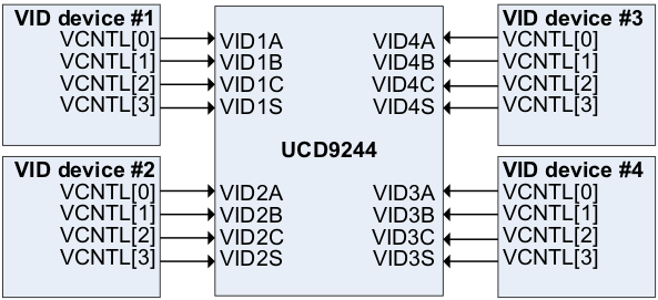
8.3.3 VID Interface
The UCD9244 supports VID (Voltage Identification) inputs from up to four external VID enabled devices. The VID codes may be 4-, 6-, or 8-bit values; the format is selected using the VID_CONFIG PMBus command. In 4- and 6-bit mode, each host uses four VID input signals (VID_A, VID_B, VID_C, and VID_S) to send VID codes to the UCD9244. In 8-bit mode, the PMBus input is used to receive VID commands from the VID devices’ I2C interfaces.
Regardless of which VID mode is used, the commanded output voltage reference is set according to this formula:
where
and
The VID_Vout_High, VID_Vout_Low, and VID_Format values are set using the VID_CONFIG PMBus command. The same command is used to set the initial VID code that will be used at power-up. In addition, the VID_CONFIG command also sets the initial voltage that the device ramps to at the end of the soft start; and defines a lockout interval over which the VID is ignored during the soft start.
VID Lockout Interval: Because the VID signals may be originating from a device that is being powered by the UCD9244, the voltage levels on the VID signal may not be valid logic levels until the supply voltage at the powered device has stabilized. For this reason a configurable lockout interval is applied each time the regulated output voltage is turned on. The lockout interval timer starts when the output voltage reaches the top of the soft-start ramp. Positive values range from 1 to 32767 ms, with 1 ms resolution. A value of 0 will enable the VID inputs immediately at the top of the start ramp. Negative values disable the lockout, allowing the VID inputs to remain active all the time regardless of the output voltage state. The default value is 0.
8.3.4 Jtag Interface
The JTAG interface can provide an alternate interface for programming the device. Four of the JTAG terminals on the UD9244 (TMS, TDI, TDO, and TCK) are shared with other functions (VID4A, VID4B, VID4C, and Syncln). JTAG is disabled by default. There are three conditions under which the JTAG interface is enabled:
- When the ROM_MODE PMBus command is issued.
- On power-up if the Data Flash is blank. This allows JTAG to be used for writing the configuration parameters to a programmed device with no PMBus interaction.
- When an invalid address is detected at power-up. By opening or shorting one of the address terminals to ground, an invalid address can be generated that enables JTAG.
When the JTAG port is enabled the shared terminals are not available for use as Syncln or VID terminals.
If JTAG is to be used, an external mechanism such as jumpers or a mux must be used to prevent conflict between JTAG and the Syncln or VID terminals.
8.3.5 Bias Supply Generator (Shunt Regulator Controller)
The I/O and analog circuits in the UCD9244 require 3.3V to operate. This can be provided using a stand-alone external 3.3V supply, or it can be generated from the main input supply using an internal shunt regulator and an external transistor. Regardless of which method is used to generate the 3.3V supply, bypass capacitors of 0.1 µF and 4.7 µF should be connected from V33A and V33D to ground near the device. An additional bypass capacitor from 0.1 to 1 µF must be connected from the BPCap terminal to ground for the internal 1.8V supply to the device’s logic circuits.
Figure 6 shows a typical application using the external transistor. The base of the transistor is driven by a resistor R1 to Vin and a transconductance amplifier whose output is on the V33FB terminal. The NPN emitter becomes the 3.3V supply for the chip.
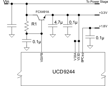 Figure 6. 3.3V Shunt Regulator Controller I/O
In order to generate the correct voltage on the base of the external pass transistor, the internal transconductance amplifier sinks current into the V33FB terminal and a voltage is produced across R1. This resistor value should be chosen so that ISINK is in the range from 0.2 to 0.4mA. R1 is defined as
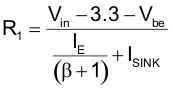
Where ISINK is the current into the V33FB terminal; Vin is the power supply input voltage, typically 12V; IE is the current draw of the device and any pull up resistors tied to the 3.3V supply; and β is the beta of the pass transistor. For ISINK = 0.3 mA, Vin=12V, β=99, Vbe = 0.7V and IE=50mA, this formula selects R1 = 10kΩ. Weaker transistors or larger current loads will require less resistance to maintain the desired ISINK current. For example, lowering β to 40 would require R1 = 5.23 kΩ; likewise, an input voltage of 5V requires a value of 1.24 kΩ for R1.
8.3.6 Power-On Reset
The UCD9244 has an integrated power-on reset (POR) circuit that monitors the supply voltage. At power-up, the POR circuit detects the V33D rise. When V33D is greater than VRESET, the device initiates an internal startup sequence. At the end of the startup sequence, the device begins normal operation, as defined by the downloaded device PMBus configuration.
8.3.7 External Reset
The device can be forced into the reset state by an external circuit connected to the nRESET terminal. A logic low voltage on this terminal holds the device in reset. To avoid an erroneous trigger caused by noise, a 10kΩ pull up resistor to 3.3V is recommended.
8.3.8 ON_OFF_CONFIG
The ON_OFF_CONFIG command is used to select the method of turning rails on and off. It can be configured so that the rail:
- stays off,
- turns on automatically,
- responds to the PMBus_Cntrl terminal,
- responds to OPERATION command, or
- responds to logical-AND of the PMBus_Cntrl terminal and the OPERATION command.
The ON_OFF_CONFIG command also sets the active polarity of the PMBus_Cntrl terminal.
8.3.9 Output Voltage Adjustment
The output voltage may be set to maintain a steady voltage or it may be controlled dynamically by the VID interface, depending on the VID_CONFIG setting. When not being commanded by the VID interface, the nominal output voltage is programmed by a combination of PMBus settings: VOUT_COMMAND, VOUT_CAL_OFFSET, VOUT_SCALE_LOOP, and VOUT_MAX. Their relationship is shown in Figure 7. These PMBus parameters need to be set such that the resulting Vref DAC value does not exceed the maximum value of Vref.
Output voltage margining is configured by the VOUT_MARGIN_HIGH and VOUT_MARGIN_LOW commands. The OPERATION command selects between the nominal output voltage and either of the margin voltages. The OPERATION command also includes an option to suppress certain voltage faults and warnings while operating at the margin settings.
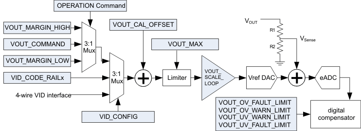 Figure 7. PMBus Voltage Adjustment Mechanisms
For a complete description of the commands supported by the UCD9244 see the UCD92xx PMBUS Command Reference (SLUU337). Each of these commands can also be issued from the Texas Instruments Fusion Digital Power™ Designer program. This Graphical User Interface (GUI) PC program issues the appropriate commands to configure the UCD9244 device.
8.3.10 Calibration
To optimize the operation of the UCD9244, PMBus commands are supplied to enable fine calibration of output voltage, output current, and temperature measurements. The supported commands and related calibration formulas may be found in the UCD92xx PMBUS Command Reference (SLUU337).
8.3.11 Analog Front End (AFE)
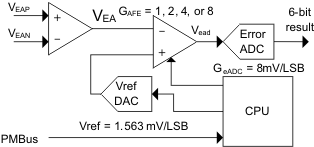 Figure 8. Analog Front End Block Diagram
The UCD9244 senses the power supply output voltage differentially through the EAP and EAN terminals. The error amplifier utilizes a switched capacitor topology that provides a wide common mode range for the output voltage sense signals. The fully differential nature of the error amplifier also ensures low offset performance.
The output voltage is sampled at a programmable time (set by the EADC_SAMPLE_TRIGGER PMBus command). When the differential input voltage is sampled, the voltage is captured in internal capacitors and then transferred to the error amplifier where the value is subtracted from the set-point reference which is generated by the 10-bit Vref DAC as shown in Figure 8. The resulting error voltage is then amplified by a programmable gain circuit before the error voltage is converted to a digital value by the error ADC (EADC). This programmable gain is configured through the PMBus and affects the dynamic range and resolution of the sensed error voltage as shown in Table 2. The internal reference gains and offsets are factory-trimmed at the 4x gain setting, so it is recommended that this setting be used whenever possible.
Table 2. Analog Front End Resolution
| AFE_GAIN for PMBus Command |
AFE Gain | EFFECTIVE ADC RESOLUTION (mV) |
DIGITAL ERROR VOLTAGE DYNAMIC RANGE (mV) |
|---|---|---|---|
| 0 | 1x | 8 | –256 to 248 |
| 1 | 2x | 4 | –128 to 124 |
| 2 (Recommended) | 4x | 2 | –64 to 62 |
| 3 | 8x | 1 | –32 to 31 |
The AFE variable gain is one of the compensation coefficients that are stored when the device is configured by issuing the CLA_GAINS PMBus command. Compensator coefficients are arranged in several banks: one bank for start/stop ramp or tracking, one bank for normal regulation mode and one bank for light load mode. This allows the user to trade-off resolution and dynamic range for each operational mode.
The EADC, which samples the error voltage, has high accuracy, high resolution, and a fast conversion time. However, its range is limited as shown in Table 2. If the output voltage is different from the reference by more than this, the EADC reports a saturated value at –32 LSBs or 31 LSBs. The UCD9244 overcomes this limitation by adjusting the Vref DAC up or down in order to bring the error voltage out of saturation. In this way, the effective range of the ADC is extended. When the EADC saturates, the Vref DAC is slewed at a rate of 0.156 V/ms, referred to the EA differential inputs.
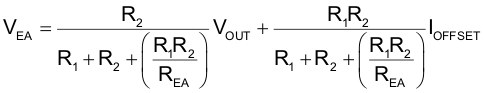
The differential feedback error voltage is defined as VEA = VEAP – VEAN. An attenuator network using resistors R1 and R2 (Figure 9) should be used to ensure that VEA does not exceed the maximum value of Vref when operating at the commanded voltage level. The commanded voltage level is determined by the PMBus settings described in the Output Voltage Adjustment section.
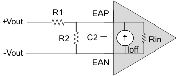 Figure 9. Input Offset Equivalent Circuit
8.3.12 Voltage Sense Filtering
Conditioning should be provided on the EAP and EAN signals. Figure 9 shows a divider network between the output voltage and the voltage sense input to the controller. The resistor divider is used to bring the output voltage within the dynamic range of the controller. When no attenuation is needed, R2 can be left open and the signal conditioned by the low-pass filter formed by R1 and C2.
As with any power supply system, maximize the accuracy of the output voltage by sensing the voltage directly across an output capacitor as close to the load as possible. Route the positive and negative differential sense signals as a balanced pair of traces or as a twisted pair cable back to the controller. Put the divider network close to the controller. This ensures that there is low impedance driving the differential voltage sense signal from the voltage rail output back to the controller. The resistance of the divider network is a trade-off between power loss and minimizing interference susceptibility. A parallel resistance (Rp) of 1kΩ to 4kΩ is a good compromise. Once RP is chosen, R1 and R2 can be determined from the following formulas.
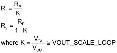
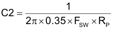
It is recommended that a capacitor be placed across the lower resistor of the divider network. This acts as an additional pole in the compensation and as an anti-alias filter for the EADC. To be effective as an anti-alias filter, the corner frequency should be 35% to 40% of the switching frequency. Then the capacitor is calculated as:
To obtain the best possible accuracy, the input resistance and offset current on the device should be considered when calculating the gain of a voltage divider between the output voltage and the EA sense inputs of the UCD9244. The input resistance and input offset current are specified in the parametric tables in this datasheet. VEA = VEAP – VEAN in the equation below.
The effect of the offset current can be reduced by making the resistance of the divider network low.
8.3.13 DPWM Engine
The output of the compensator feeds the high resolution DPWM engine. The DPWM engine produces the pulse width modulated gate drive output from the device. In operation, the compensator calculates the necessary duty cycle as a digital number representing a percentage from 0 to 100%. The duty cycle value is multiplied by the configured period to generate a comparator threshold value. This threshold is compared against the high speed switching period counter to generate the desired DPWM pulse width. This is shown in Figure 10.
Each DPWM engine can be synchronized to another DPWM engine or to an external sync signal via the SyncIn and SyncOut terminals. Configuration of the synchronization function is done through a MFR_SPECIFIC PMBus command. See the DPWM Synchronization section for more details.
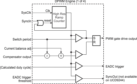 Figure 10. DPWM Engine
8.3.14 Rail/Power Stage Configuration
Unlike many other products in the UCD92xx family, the UCD9244 does not support assigning power stages to arbitrary rails, or combining multiple power stages on the same rail. The UCD9244 supports up to two single-phase rails, and the channel number of each rail’s DPWM output must match that of its EAP/EAN feedback inputs.
8.3.15 DPWM Phase Synchronization
DPWM synchronization provides a method to link the timing between voltage rails controlled by the UCD92xx device--either internally or between devices. The configuration of the synchronization between rails is performed by the issuing the SYNC_CONFIG command. For details of issuing this command, see the UCD92xx PMBUS Command Reference (SLUU337). The synchronization behavior can also be configured using the Fusion Digital Power Designer software. Below is a summary of the function.
Each digital pulse width modulator (PWM) engine in the UCD92xx controller can accept a sync signal that resets the PWM ramp generator. The ramp generator can be set to free-run, accept a reset signal from another internal PWM engine, or accept a reset signal from the external SyncIn terminal. In this way the PWM timers can be "daisy-chained" to set up the desired phase relationship between power stages.
The PWM engine reset input can accept the following inputs
Table 3. Sync Trigger Inputs
| SYNC SIGNAL |
|---|
| None (free run) |
| DPWM 1 |
| DPWM 2 |
| DPWM 3 |
| DPWM 4 |
| SyncIn terminal |
Table 4. Available Source For SyncOut
| SYNC SIGNAL |
|---|
| Disabled |
| DPWM 1 |
| DPWM 2 |
| DPWM 3 |
| DPWM 4 |
When configuring a PWM engine to run synchronous to another internal PWM output, set the switching frequency of each PWM output to the same value using the FREQUENCY_SWITCH PMBus command. Set the time point where the controller samples the voltage to be regulated by setting the EADC_SAMPLE_TRIGGER value to the minimum value (228-240 nsec before the end of the switching period).
When configuring a PWM engine to run synchronous to an external sync signal, the switching period must be set to be longer than the period of the sync signal by setting the value of the FREQUENCY_SWITCH command to be lower than the frequency of the sync signal. This way the external sync signal will reset the PWM ramp counter before it is internally reset. In this operating condition, the error ADC sample trigger time must be set to:
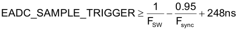
where Fsw is the switching frequency set by FREQUENCY_SWITCH and Fsync is the minimum synchronization frequency. The factor of 0.95 is due to the 5% tolerance on the internal clock in the controller. This will ensure that the regulation voltage is sampled "just in time" to calculate the appropriate control effort for each switching period. This is shown in Figure 11.
 Figure 11. Relationship Of EADC Trigger To External Sync
If two rails share a common sync source other than the SyncIn terminal, they must have the same delay. When the SyncIn terminal is used as a sync source, the delay is applied using a different register (EV1) than when using the other sources (which use the PhaseTrig registers). Using the EV1 register introduces delay in the control loop calculation that will introduce phase loss that must be taken into consideration when calculating the loop compensation. Therefore, under most conditions it will be desirable to set the delay to zero for the PWM signal synchronized by the SyncIn terminal.
8.3.16 Output Current Measurement
Terminals CS1A, CS2A, CS3A, and CS4A are used to measure either output current or inductor current in each of the controlled power stages. PMBus commands IOUT_CAL_GAIN and IOUT_CAL_OFFSET are used to calibrate each measurement. See the UCD92xx PMBus Command Reference (SLUU337) for specifics on configuring this voltage to current conversion.
When the measured current is outside the range of either the over-current or under-current fault threshold, a current limit fault is declared and the UCD9244 performs the PMBus configured fault recovery. ADC current measurements are digitally averaged before they are compared against the over-current and under-current warning and fault thresholds. The output current is measured at a rate of one output rail per tIout microseconds. The current measurements are then passed through a digital smoothing filter to reduce noise on the signal and prevent false errors. The output of the smoothing filter asymptotically approaches the input value with a time constant that is approximately 3.5 times the sampling interval.
Table 5. Output Current Filter Time Constants
| NUMBER OF OUTPUT RAILS |
OUTPUT CURRENT SAMPLING INTERVALS (µs) |
FILTER TIME CONSTANT τ (ms) |
|---|---|---|
| 1 | 200 | 0.7 |
| 2 | 400 | 1.4 |
| 3 | 600 | 2.1 |
| 4 | 800 | 2.8 |
This smoothed current measurement is used for output current fault detection; see the Over-Current Detection section. The smoothed current measurement is also reported in response to a PMBus request for a current reading.
8.3.17 Current Sense Input Filtering
Each power stage current is monitored by the device at the CS terminals. The device monitors the current with a 12-bit ADC and also monitors the current with a digitally programmable analog comparator. The comparator can be disabled by writing a zero to the FAST_OC_FAULT_LIMIT.
Because the current sense signal is both digitally sampled and compared to the programmable over-current threshold, it should be conditioned with an RC network acting as an anti-alias filter. If the comparator is disabled, the CS input should be filtered at 35% of the sampling rate. An RC network with this characteristic can be calculated as
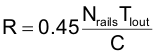
where Nrails is the number of rails configured and TIout is the sample period for the current sense inputs. Therefore, when the comparator is not used, the recommended component values for the RC network are C = 10 nF and R = 35.7 kΩ.
When the fast over-current comparator is used, the filter corner frequency based on the ADC sample rate may be too slow and a corner frequency that is a compromise between the requirements of fast over-current detection and attenuating aliased content in the sampled current must be sought. In this case, the filter corner frequency can be calculated based on the time to cross the over-current threshold.
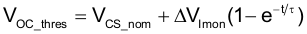
where VOC_thres is the programmed OC comparator threshold, VCS_nom is the nominal CS voltage, ΔVImon is the change in CS voltage due to an over-current fault and τ is the filter time constant. Using the equation for the comparator voltage above, the RC network values can be calculated as
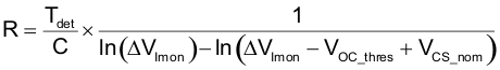
where Tdet is the time to cross the over-current comparator threshold. For Tdet = 10 µs, ΔVImon = 1.5V, VOC_thres = 2.0V and VCS_nom = 1.5V, the corner frequency is 6.4 kHz and the recommended RC network component values are C = 10 nF and R = 2.49 kΩ.
8.3.18 Over-Current Detection
Several mechanisms are provided to sense output current fault conditions. This allows for the design of power systems with multiple layers of protection.
- Integrated gate drivers such as the UCD72xx family can be used to generate the FLT signal. The driver monitors the voltage drop across the high side FET and if it exceeds a resistor/voltage programmed threshold, the driver activates its fault output. A logic high signal on the FLT input causes a hardware interrupt to the internal CPU, which then disables the DPWM output. This process takes about 14 microseconds.
- Inputs CS1A, CS2A, CS3A, and CS4A each drive an internal analog comparator. These comparators can be used to detect the voltage output of a current sense circuit. Each comparator has a separate threshold that can be set by the FAST_OC_FAULT_LIMIT PMBus command. Though the command is specified in amperes, the hardware threshold is programmed with a value between 31mV and 2V in 64 steps. The relationship between amperes to sensed volts is configured by the IOUT_CAL_GAIN command. When the current sense voltage exceeds the threshold, the corresponding DPWM output is driven low on the voltage rail with the fault.
- Each Current Sense input to the UCD9244 is also monitored by the 12-bit ADC. Each measured value is scaled using the IOUT_CAL_GAIN and IOUT_CAL_OFFSET commands and then passed through a digital smoothing filter. The smoothed current measurements are compared to fault and warning limits set by the IOUT_OC_FAULT_LIMIT and IOUT_OC_WARN_LIMIT commands. The action taken when an OC fault is detected is defined by the IOUT_OC_FAULT_RESPONSE command.
Because the current measurement is averaged with a smoothing filter, the response time to an over-current condition depends on a combination of the time constant (τ) from Table 5, the recent measurement history, and how much the measured value exceeds the over-current limit. When the current steps from a current (I1) that is less than the limit to a higher current (I2) that is greater than the limit, the output of the smoothing filter is
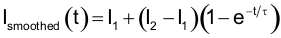
At the point when Ismoothed exceeds the limit, the smoothing filter lags time, tlag is
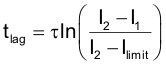
The worst case response time to an over-current condition is the sum of the sampling interval (Table 5) and the smoothing filter lag, tlag from Equation 13.
8.3.19 Input Voltage Monitoring
The VinMon terminal on the UCD9244 monitors the input voltage. The VinMon terminal is monitored using the internal 12-bit ADC which has a dynamic range of 0 to 2.5V. The fault thresholds for the input voltage are set using the VIN_OV_FAULT_LIMIT and VIN_UV_FAULT_LIMIT commands. The scaling for Vin is set using the VIN_SCALE_MONITOR command.
8.3.20 Input UV Lockout
The input supply lock-out voltage thresholds are configured with the VIN_ON and VIN_OFF commands. When input supply voltage drops below the value set by VIN_OFF, the device starts a normal soft stop ramp. When the input supply voltage drops below the voltage set by VIN_UV_FAULT_LIMIT, the device performs as configured by the VIN_UV_FAULT_RESPONSE command. For example, when the bias supply for the controller is derived from another source, the response code can be set to "Continue" or "Continue with delay," and the controller attempts to finish the soft stop ramp. If the bias voltages for the controller and gate driver are uncertain below some voltage, the user can set the UV fault limit to that voltage and specify the response code to be "shut down immediately," disabling all DPWM outputs. VIN_OFF sets the voltage at which the output voltage soft-stop ramp is initiated, and VIN_UV_FAULT_LIMIT sets the voltage where power conversion is stopped.
8.3.21 Temperature Monitoring
The UCD9244 monitors temperature using the 12-bit ADC. The ADC12 is read every 100us and combined into a running sum. At the end of each 100ms monitoring interval, the ~1000 sample in the running sum are averaged together and the running sum is restarted. These averaged values are used to calculate the temperature from external temperature sensors. These same values may be read directly using the READ_AUX_ADCS PMBus command.
The averaged values are passed through an additional digital smoothing filter to further reduce the chance of reporting false over-temperature events. The smoothing filter has a time constant of 1.55 seconds.
8.3.22 Auxiliary ADC Input Monitoring
Unused external temperature sensor inputs may be used for general-purpose analog monitoring. The READ_AUX_ADCS PMBus command returns a block of four 16-bit values, each of which is the average of multiple raw measurements from the Temp/AuxADC inputs. A value of 0 corresponds to 0.00V and a value of 65535 corresponds to 2.50V. Unlike many other variables that can be monitored via PMBus, no mechanism is provided for adjusting the gain or offset of the Aux ADC measurements.
When using the temperature sensor inputs as Auxiliary ADCs, the temperature warning and faults should be disabled to prevent shut-downs due to non-existent over-temperature conditions.
8.3.23 Soft Start, Soft Stop Ramp Sequence
The UCD9244 performs soft start and soft stop ramps under closed-loop control.
Performing a start or stop ramp or tracking is considered a separate operational mode. The other operational modes are normal regulation and light load regulation. Each operational mode can be configured to have an independent loop gain and compensation. Each set of loop gain coefficients is called a "bank" and is configured using the CLA_GAINS PMBus command.
Start ramps are performed by waiting for the configured start delay TON_DELAY and then ramping the internal reference toward the commanded reference voltage at the rate specified by the TON_RISE time and VOUT_COMMAND. The DPWM outputs are enabled when the internal ramp reference equals the preexisting voltage (pre-bias) on the output and the calculated DPWM pulse width exceeds the pulse width specified by DRIVER_MIN_PULSE. This ensures that a constant ramp rate is maintained, and that the ramp is completed at the same time it would be if there had not been a pre-bias condition.
Figure 12 and Figure 13 show the operation of soft-start and soft-stop ramps.
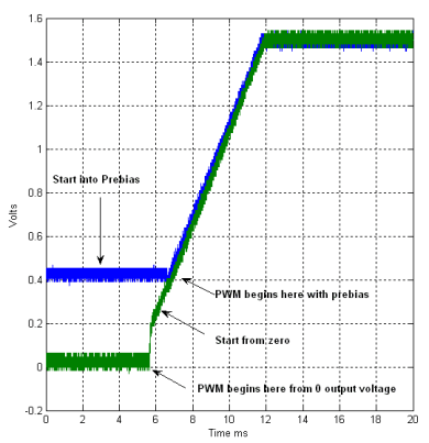 Figure 12. Soft-Start Ramp
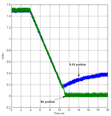 Figure 13. Soft-Stop Ramp
When a voltage rail is in its idle state, the DPWM outputs are disabled, and the differential voltage on the EAP/EAN terminals are monitored by the controller. During idle the Vref DAC is adjusted to match the feedback voltage. If there is a pre-bias (that is, a non-zero voltage on the regulated output), then the device can begin the start ramp from that voltage with a minimum of disturbance. This is done by calculating the duty cycle that is required to match the measured voltage on the rail. Nominally this is calculated as Vout / Vin. If the pre-bias voltage on the output requires a smaller pulse width than the driver can deliver, as defined by the DRIVER_MIN_PULSE PMBus command, then the start ramp is delayed until the internal ramp reference voltage has increased to the point where the required duty cycle exceeds the specified minimum duty.
Once a soft start/stop ramp has begun, the output is controlled by adjusting the Vref DAC at a fixed rate and allowing the digital compensator control engine to generate a duty cycle based on the error. The Vref DAC adjustments are made at a rate of 10 kHz and are based on the TON_RISE or TOFF_FALL PMBus configuration parameters.
Although the presence of a pre-bias voltage or a specified minimum DPWM pulse width affects the time when the DPWM signals become active, the time from when the controller starts processing the turn-on command to the time when it reaches regulation is TON_DELAY plus TON_RISE, regardless of the pre-bias or minimum duty cycle.
During a normal ramp (i.e. no tracking, no current limiting events and no EADC saturation), the set point slews at a pre-calculated rate based on the commanded output voltage and TON_RISE. Under closed loop control, the compensator follows this ramp up to the regulation point.
Because the EADC in the controller has a limited range, it may saturate due to a large transient during a start/stop ramp. If this occurs, the controller overrides the calculated set point ramp value, and adjusts the Vref DAC in the direction to minimize the error. It continues to step the Vref DAC in this direction until the EADC comes out of saturation. Once it is out of saturation, the start ramp continues, but from this new set point voltage; and therefore, has an impact on the ramp time.
8.3.24 Non-Volatile Memory Error Correction Coding
The UCD9244 uses Error Correcting Code (ECC) to improve data integrity and provide high reliability storage of Data Flash contents. ECC uses dedicated hardware to generate extra check bits for the user data as it is written into the Flash memory. This adds an additional six bits to each 32-bit memory word stored into the Flash array. These extra check bits, along with the hardware ECC algorithm, allow for any single bit error to be detected and corrected when the Data Flash is read.
8.3.25 Data Logging
The UCD9244 maintains a data log in non-volatile memory. This log tracks the peak internal and external temperature sensor measurements, peak current measurements and fault history. The PMBus commands and data format for the Data Logging can be found in the UCD92xx PMBus Command Reference (SLUU337).
8.4 Device Functional Modes
8.4.1 4-Bit VID Mode
In 4-bit VID mode, the four VID input signals are used to provide the four bits of VID data, as shown in the table below. The VID lines are level-sensitive, and are periodically polled every 400µs. When the VID lines are changed to command a new voltage, there may be a delay of 500 to 600µs while the UCD9244 confirms that the VID signal levels are stable. The output voltage will then slew to the new setpoint voltage at the rate specified by the PMBus VOUT_TRANSITION_RATE command.
| TERMINAL | PURPOSE | RAIL 1 | RAIL 2 | RAIL 3 | RAIL 4 |
|---|---|---|---|---|---|
| VID_A | Data bit 0 (least significant bit) | VID1A | VID2A | VID3A | VID4A |
| VID_B | Data bit 1 | VID1B | VID2B | VID3B | VID4B |
| VID_C | Data bit 2 | VID1C | VID2C | VID3C | VID4C |
| VID_S | Data bit 3 (most significant bit) | VID1S | VID2S | VID3S | VID4S |
8.4.2 6-Bit VID Mode
In 6-bit VID mode, the four VID input signals are used to provide the six bits of VID data, as shown in the table below. Each of the three data lines (VID_A, VID_B, and VID_C) carries two bits of data per VID code. The bits are clocked and selected by the VID_S select line.
| TERMINAL | PURPOSE | RAIL 1 | RAIL 2 | RAIL 3 | RAIL 4 |
|---|---|---|---|---|---|
| VID_A | Data bit 0 when VID_S is low, Data bit 3 when VID_S is high |
VID1A | VID2A | VID3A | VID4A |
| VID_B | Data bit 1 when VID_S is low, Data bit 4 when VID_S is high |
VID1B | VID2B | VID3B | VID4B |
| VID_C | Data bit 2 when VID_S is low, Data bit 5 when VID_S is high |
VID1C | VID2C | VID3C | VID4C |
| VID_S | Select Line: Low= LSB, High = MSB |
VID1S | VID2S | VID3S | VID4S |
The falling edge of the VID_S line triggers the UCD9244 to read bits 2:0 on the three VID data lines. The rising edge of VID_S triggers the UCD9244 to read bits 5:3 on the three VID data lines and calculate a new VOUT setpoint. This calculation takes from 35 to 135µs. The output voltage will then slew to the new setpoint voltage at the rate specified by the VOUT_TRANSITION_RATE PMBus command.
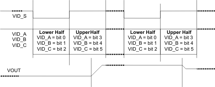 Figure 14. 6-Bit VID Data Transfer
The set-up time on the data lines is 0 µs. All four VID lines must hold at the same level for some time after a change in the VID_S line to allow the UCD9244 to read and validate the data signals and perform necessary voltage calculations. The UCD9244 can tolerate single hold times as short as 70µs, but does not have sufficient computation power to sustain continuous VID messaging that quickly. It is expected that the hold time will be at least 125µs for sustained operations. It is recommended that the DSP only send VID messages when the regulated voltage needs to change; sending the same VID code repeatedly and continuously provides no benefit.
Figure 15 and Table 6 illustrate the critical timing measurements as they apply to the 6-bit VID interface.
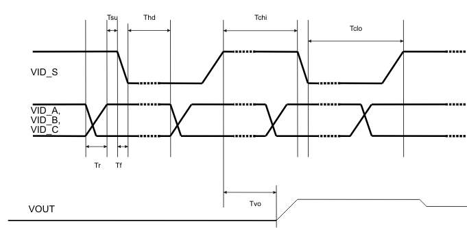 Figure 15. 6-Bit VID Timing
Table 6. 6-Bit VID Timing
| SYMBOL | PARAMETER | MIN | TYP | MAX | UNITS |
|---|---|---|---|---|---|
| Tr | Data and clock rise time | – | 2.5 | µs | |
| Tf | Data and clock fall time | – | 0.3 | µs | |
| Tsu | Data setup before changing clock | 0 | µs | ||
| Thd | Data hold until next clock change | 70 | µs | ||
| Tchi | Clock high time | 70 | 125 | µs | |
| Tclo | Clock low time | 70 | 125 | µs | |
| Tvo | Response time from rising edge of VID_S to start of Vout slewing to new setpoint | 35 | 135 | µs |
8.4.3 8-Bit VID Mode
In 8-bit VID mode, the four VID input signals are not used. Instead, an 8-bit VID code is transmitted to the UCD9244 through the PMBus / I2C port using one of the VID_CODE_RAILn commands, where n is the rail number from 1 to 4.
| NAME | DESCRIPTION(1) | CODE |
|---|---|---|
| VID_CONFIG | Selects the VID mode, sets the upper and lower voltage limits, and the starting voltage code at power-up. | 0xBB |
| VID_CODE_RAIL1 | Selects the VID code used to set the output voltage for Rail 1. | 0xBC |
| VID_CODE_RAIL2 | Selects the VID code used to set the output voltage for Rail 2. | 0xBD |
| VID_CODE_RAIL3 | Selects the VID code used to set the output voltage for Rail 3. | 0xBE |
| VID_CODE_RAIL4 | Selects the VID code used to set the output voltage for Rail 4. | 0xBF |
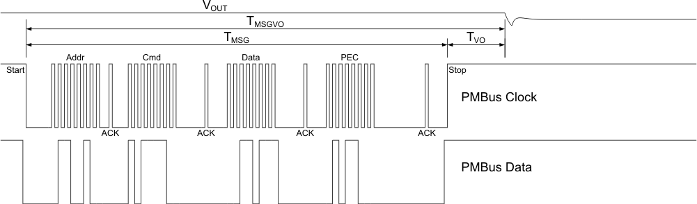 Figure 16. PMBus Timing For VID_CODE_RAILn Command
Table 7. Typical PMBus Timing For VID_CODE_RAILn Command at 400kHz
| SYMBOL | PARAMETER | CONDITIONS | TYP | UNITS |
|---|---|---|---|---|
| TmsgPEC | Message Transmit Time, with PEC | 400 kHz clock, PEC enabled | 162 – 256 | µs |
| Message Transmit Time, without PEC | 400 kHz clock, PEC enabled | 126 – 221 | ||
| Tvo | End of message until Vout starts changing | 28 – 140 | µs | |
| Tmsgvo | Start of message until Vout start changing | 400 kHz clock, PEC disabled | 169 – 314 | µs |
The total time to transmit the serial VID command will vary depending on the other tasks that the UCD92xx processor is performing. Typical packet times varied from 162 to 256µs when the PMBus is configured for a 400 kb/s transfer rate running and the optional PEC byte is enabled. Disabling the PEC byte saves about 35µs and the transfer times are from 126 to 221µs. Note that these are not specified best-case/worst-case timings, but indicate a range given the typical acknowledge overhead in the host and controller.
After the VID packet has been received by the controller there is a delay before the set-point reference DAC is updated. This delay time varies from ~28µs to 140µs (typical ) depending on the existing priority of updating set-point reference DAC when the command is received.
With a 221µs packet transfer time, it would seem possible to send 4500 VID messages per second to the device. Very short bursts at this rate might be acceptable, but doing so for sustained periods could overwhelm the available processing resources in the UCD92xx, causing it to be delayed in performing its other monitoring and fault response tasks. In addition, if multiple hosts are trying to talk on the PMBus at such high rates then bus contention will occur with great regularity.
To prevent these issues, it is prudent to limit the total VID messaging rate to less than 4 messages per millisecond. In a system with four independent hosts, each host might need to be limited to less than 1 message per millisecond. Therefore, to minimize PMBus traffic, it is best to only issue the VID command when a voltage change is required. There is no benefit to sending the same VID code continuously and repeatedly.
8.4.4 Current Foldback Mode
When the measured output current exceeds the value specified by the IOUT_OC_FAULT_LIMIT command, the UCD9244 attempts to continue to operate by reducing the output voltage in order to maintain the output current at the value set by IOUT_OC_FAULT_LIMIT. This continues indefinitely as long as the output voltage remains above the minimum value specified by IOUT_OC_LV_FAULT_LIMIT. If the output voltage is pulled down to less than that value, the device responds as programmed by the IOUT_OC_LV_FAULT_RESPONSE command.