SLUSFA7 July   2025 UCC57142 , UCC57148

PRODUCTION DATA  

  1.   1
  2. 1Features
  3. 2Applications
  4. 3Description
  5. 4Pin Configuration and Functions
  6. 5Specifications
    1. 5.1 Absolute Maximum Ratings
    2. 5.2 ESD Ratings
    3. 5.3 Recommended Operating Conditions
    4. 5.4 Thermal Information
    5. 5.5 Electrical Characteristics
    6. 5.6 Switching Characteristics
    7. 5.7 Timing Diagram
    8. 5.8 Typical Characteristics
  7. 6Detailed Description
    1. 6.1 Overview
    2. 6.2 Functional Block Diagram
    3. 6.3 Feature Description
      1. 6.3.1 Input Stage
      2. 6.3.2 Enable/Fault (EN/FLT)
      3. 6.3.3 Driver Stage
      4. 6.3.4 Over Current (OC) Protection
      5. 6.3.5 Thermal Shutdown
    4. 6.4 Device Functional Modes
  8. 7 Applications and Implementation
    1. 7.1 Application Information
    2. 7.2 Typical Application
      1. 7.2.1 Driving MOSFET/IGBT/SiC MOSFET
        1. 7.2.1.1 Design Requirements
        2. 7.2.1.2 Detailed Design Procedure
          1. 7.2.1.2.1 VDD Undervoltage Lockout
          2. 7.2.1.2.2 Power Dissipation
        3. 7.2.1.3 Application Curves
    3. 7.3 Power Supply Recommendations
    4. 7.4 Layout
      1. 7.4.1 Layout Guidelines
      2. 7.4.2 Layout Example
      3. 7.4.3 Thermal Consideration
  9. 8Revision History
  10. 9Mechanical, Packaging, and Orderable Information

封装选项

请参考 PDF 数据表获取器件具体的封装图。

机械数据 (封装 | 引脚)
  • DBV|6
散热焊盘机械数据 (封装 | 引脚)
订购信息

Typical Characteristics

Unless otherwise specified, VDD=15V, IN=3.3V, EN=5V, TJ = 25 °C, No load

UCC57142 UCC57148 Quiescent Current
VDD = 6.5V
Figure 5-2 Quiescent Current
UCC57142 UCC57148 Disable Current
Figure 5-4 Disable Current
UCC57142 UCC57148 UVLO Threshold Figure 5-6 UVLO Threshold
UCC57142 UCC57148 Input Pulldown ResistanceFigure 5-8 Input Pulldown Resistance
UCC57142 UCC57148 Enable Pullup
                        ResistanceFigure 5-10 Enable Pullup Resistance
UCC57142 UCC57148 Output Pulldown Resistance Figure 5-12 Output Pulldown Resistance
UCC57142 UCC57148 Output Fall Time
CLOAD = 1.8nF
Figure 5-14 Output Fall Time
UCC57142 UCC57148 Input
                        to Output Rising (Turnon) Propagation Delay
CLOAD = 1.8nF
Figure 5-16 Input to Output Rising (Turnon) Propagation Delay
UCC57142 UCC57148 Input Propagation Delay
CLOAD = 1.8nF
Figure 5-18 Input Propagation Delay
UCC57142 UCC57148 OC
                        Threshold Figure 5-20 OC Threshold
UCC57142 UCC57148 OC to
                        Fault Propagation DelayFigure 5-22 OC to Fault Propagation Delay
UCC57142 UCC57148 Operating Static Supply Current
Figure 5-3 Operating Static Supply Current
UCC57142 UCC57148 Operating Supply Current
CLOAD = 1.8nF
Figure 5-5 Operating Supply Current
UCC57142 UCC57148 Input Threshold Figure 5-7 Input Threshold
UCC57142 UCC57148 Enable Threshold Figure 5-9 Enable Threshold
UCC57142 UCC57148 Output Pullup Resistance vs VDDFigure 5-11 Output Pullup Resistance vs VDD
UCC57142 UCC57148 Output Rise Time
CLOAD = 1.8nF
Figure 5-13 Output Rise Time
UCC57142 UCC57148 Output Rise and Fall Time
CLOAD = 1.8nF
Figure 5-15 Output Rise and Fall Time
UCC57142 UCC57148 Input
                        to Output Falling (Turnoff) Propagation Delay
CLOAD = 1.8nF
Figure 5-17 Input to Output Falling (Turnoff) Propagation Delay
UCC57142 UCC57148 Disable Propagation Delay
CLOAD = 1.8nF
Figure 5-19 Disable Propagation Delay
UCC57142 UCC57148 OC to Output Propagation
                        DelayFigure 5-21 OC to Output Propagation Delay
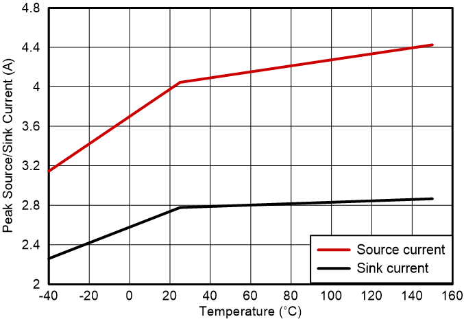
UCC57142 UCC57148 Peak
                        Source and Sink Current
CLOAD = 1μF
Figure 5-23 Peak Source and Sink Current