ZHCSCP2 July 2014 UCC28880
PRODUCTION DATA.
- 1 特性
- 2 应用
- 3 说明
- 4 修订历史记录
- 5 Pin Configuration and Functions
- 6 Specifications
- 7 Detailed Description
-
8 Application and Implementation
- 8.1 Application Information
- 8.2
Typical Application
- 8.2.1 12-V, 100-mA Low-Side Buck Converter
- 8.2.2 12-V, 100-mA, High-Side Buck Converter
- 8.2.3
Additional UCC28880 Application Topologies
- 8.2.3.1 Low-Side Buck and LED Driver - Direct Feedback (level-shifted)
- 8.2.3.2 12-V, 100-mA High-Side Buck Converter
- 8.2.3.3 Non-Isolated, Low-Side Buck-Boost Converter
- 8.2.3.4 9.5 Non-Isolated, High-Side Buck-Boost Converter
- 8.2.3.5 9.6 Non-Isolated Flyback Converter
- 8.2.3.6 Isolated Flyback Converter
- 9 Power Supply Recommendations
- 10Layout
- 11器件和文档支持
- 12机械封装和可订购信息
8 Application and Implementation
8.1 Application Information
The UCC28880 can be used in various application topologies with direct or isolated feedback. The device can be used in low-side buck, where the output voltage is negative, or as a low-side buck-boost configuration, where the output voltage is positive. In both configurations the common reference node is the positive input node (VIN+). The device can also be configured as a LED driver in either of the above mentioned configurations. If the application requires the AC-to-DC power supply output to be referenced to the negative input node (VIN-), the UCC28880 can also be configured as a traditional high-side buck as shown in Figure 17. In this configuration, the voltage feedback is sampling the output voltage VOUT, making the DC regulation less accurate and load dependent than in low-side buck configuration, where the feedback is always tracking the VOUT. However, high-conversion efficiency can still be obtained.
8.2 Typical Application
8.2.1 12-V, 100-mA Low-Side Buck Converter
Figure 14 shows a typical application example of a non-isolated power supply, where the UCC28880 is connected in a low-side buck configuration having an output voltage that is negative with respect to the positive input voltage (VIN+). The output voltage is set to 12 V in this example, but can easily be changed by changing the value of RFB1. This application can be used for a wide variety of household appliances and automation, or any other applications where mains isolation is not required.
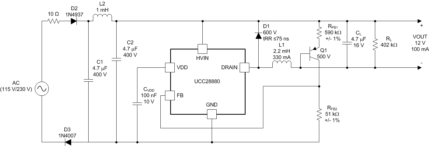 Figure 14. Universal Input, 12-V, 100-mA Output Low-Side Buck
8.2.1.1 Design Requirements
Table 1. Table 1 Design specification
| DESCRIPTION | MIN | MAX | UNIT | |
|---|---|---|---|---|
| Design Input | ||||
| VIN | AC input voltage | 85 | 265 | VRMS |
| fLINE | Line frequency | 47 | 63 | Hz |
| IOUT | Output current | 0 | 100 | mA |
| Design Requirements | ||||
| PNL | No-load input power | 50 | mW | |
| VOUT | Output voltage | 12 | 13 | V |
| ΔVOUT | Output voltage ripple | 350 | mV | |
| η | Converter efficiency | 68% | ||
8.2.1.2 Detailed Design Procedure
8.2.1.2.1 Input Stage (RF, D2, D3, C1, C2, L2)
- Resistor RF is a flame-proof fusible resistor. RF limits the inrush current, and also provide protection in case any component failure causes a short circuit. Value for its resistance is generally selected between 4.7 Ω to 15 Ω.
- A half-wave rectifier is chosen and implemented by diode D2 (1N4937). It is a general purpose 1-A, 600-V rated diode. It has a fast reverse recovery time (200 ns) for improved differential-mode-conducted EMI noise performance. Diode D3 (1N4007) is a general purpose 1-A, 1-kV rated diode with standard reverse recovery time (>500 ns), and is added for improved common-mode-conducted EMI noise performance. D3 can be removed and replaced by a short if not needed.
- EMI filtering is implemented by using a single differential-stage filter (C1-L2-C2).
Capacitors C1 and C2 in the EMI filter also acts as storage capacitors for the high-voltage input DC voltage (VIN).The required input capacitor size can be calculated according formula (1).
where
- CBULK(min) is minimum value for the total input capacitor value (C1 + C2 in the schematic of Figure 14).
- RCT = 1 in case a single wave rectifier and RCT = 2 in case of full-wave rectifier (for the schematic reported in Figure 20 RCT = 1 because of a single rectifier).
- PIN is the converter input power.
- VIN(min) is the minimum RMS value of the AC input voltage.
- VBULK(min) is the minimum allowed voltage value across bulk capacitor during converter operation.
- fLINE(min) is the minimum line frequency when the line voltage is VIN(min).
- The converter maximum output power is: POUT = IOUT x VOUT = 0.1 A x 12.5 V = 1.25 W
- Assuming the efficiency η = 68.% the input power is PIN = POUT/η = 1.765 W
- VBULK(min) = 80 V
- VIN(min) = 85 VRMS (from design specification table)
- fLINE(min) = 57 Hz
CBULK(min) = 6.96 μF. Considering that electrolytic capacitors, generally used as bulk capacitor, have 20% of tolerance in value, the minimum nominal value required for CBULK is:
Select C1 and C2 to be 4.7μF each (CBULK = 4.7 μF + 4.7 μF = 9.4 μF > CBULKn(min)).
By using a full-wave rectifier allows a smaller capacitor for C1 and C2, almost 50% smaller.
8.2.1.2.2 Regulator Capacitor (CVDD)
Capacitor CVDD acts as the decoupling capacitor and storage capacitor for the internal regulator. A 100-nF, 10-V rated ceramic capacitor is enough for proper operation of the device's internal LDO.
8.2.1.2.3 Freewheeling Diode (D1)
The freewheeling diode has to be rated for high-voltage with as short as possible reverse-recovery time (trr).
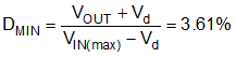
The maximum reverse voltage that the diode should experience in the application, during normal operation, is given by Equation 4.
A margin of 20% is generally considered.
The chosen freewheeling diode for the application example is a 600-V, 1-A rated diode with a trr ≤ 75 ns. It is possible to use a diode with higher trr but this leads to higher switching losses and lower efficiency.
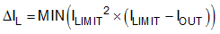
8.2.1.2.4 Inductor (L1)
Initial calculations:
Ripple current at full load:
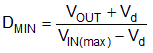
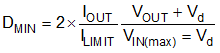
Average MOSFET conduction minimum duty cycle at full load and maximum input voltage is:
If the converter operates in continuous conduction mode:
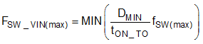
Maximum allowed switching frequency at VIN_MAX and full load:
ILIMIT = 150 mA, the worst case but assuming ΔIL = 100mA.
The converter works in continuous conduction mode (ΔIL < ILIMIT) so the
The maximum allowed switching frequency is:
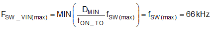
The duty cycle does not force the MOSFET on time to go below tON_TO. If DMIN/TON_TO < fSW(max), the switching frequency is reduced by current runaway protection and the maximum average switching frequency is lower than fSW(max).
The minimum inductance value satisfies both the following conditions:
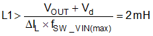

In the application example, 2.2 mH is selected as the minimum standard value that satisfy Equation 11 and Equation 12.
8.2.1.2.5 Output Capacitor (CL)
The value of the output capacitor impacts the output ripple. Depending on the combination of capacitor value and equivalent series resistor (RESR). A larger capacitor value also has an impact on the start-up time. For a typical application, the capacitor value can start from 47 μF, to hundreds of μF. A guide for sizing the capacitor value can be calculated by the following equations:
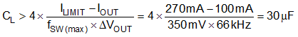
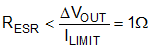
Take into account that both CL and RESR contribute to output voltage ripple. A first pass capacitance value can be selected and the contribution of CL and RESR to the output voltage ripple can be evaluated. If the total ripple is too high the capacitance value has to increase or RESR value must be reduced. In the application example CL was selected (47 µF) and it has an RESR of 0.3 Ω. So the RESR contributes for 1/3 of the total ripple. The formula that calculates CL is based on the assumption that the converter operates in burst of four switching cycles. The number of bursts per cycle could be different, the formula for CL is a first approximation.
8.2.1.2.6 Load Resistor (RL)
The resistor should be chosen so that the output current in any standby/no-load condition is higher than the leakage current through the integrated power MOSFET. If the standby load current is ensured to always be larger than the specified ILEAKAGE, the RL is not needed. If OVP protection is required for safety reasons, then a zener could be placed across the output (not fitted in the application example). In the application example RL = 402 kΩ. This ensures a minimum load current of at least ~30 µA when VOUT = 12 V.
8.2.1.2.7 Feedback Path (Q1, RFB1, RFB2)
The feedback path of Q1, RFB1 and RFB2 implements a level-shifted direct feedback. RFB2 sets the current through the feedback path, and RFB1 sets the output voltage. Q1 acts as the level shifter and needs to be rated for high voltage. The output voltage is determined as follows:
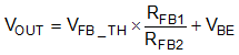
where
- VOUT is the output voltage.
- VFB_TH is the FB pin voltage threshold = VFB_TH.
- VBE is the base-Emitter saturation voltage of the external PNP transistor.
- RFB1 is the external resistor setting the output voltage (depending on the current set by RFB2, and the Vbe).
- RFB2 is the external resistor setting the current through the external feedback path.
For the application example a target of ~20-μA of current is selected through the external feedback path (IFB).
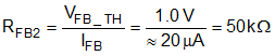
Choose a standard resistor size for RFB2 = 51 kΩ. For the high-voltage PNP transistor choose a 500-V rated transistor with a VBE ≈ 0.5 V for the feedback current. To achieve the 12-V output voltage RFB1 needs to be:
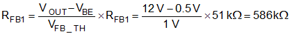
Choose a standard resistor size for RFB1 = 591 kΩ.
To change the output voltage, change the value for RFB1. For example, to target a 5-V output voltage, RFB1 should be changed to a 230-kΩ resistor.
Accuracy of the output-voltage level depends proportionally on the variation of VFB_TH, and on the absolute accuracy of VBE according to Equation 16 and Equation 17.
The current through the feedback path is connected over the high voltage input (VIN), and this feedback current is always on. Higher current provides less noise-sensitive feedback, the feedback current should be minimized in order to minimize the total power consumption.
8.2.1.3 Application Curves
Figure 15 shows the efficiency diagram of the converter, a design previous discussed. Figure 16 shows the output voltage vs output current diagram. The two diagrams were obtained by measuring efficiency (Figure 15), output current and output voltage (Figure 16) moving resistive load value from infinite (load disconnected) up to zero (output shorted). The different curves of the diagram correspond to different AC input voltage.
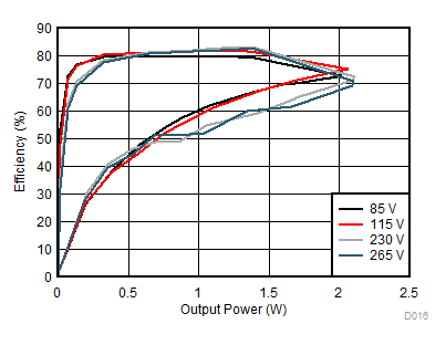 Figure 15. Efficiency vs Output Power Diagrams
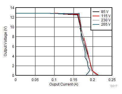 Figure 16. Output Voltage vs Output Current Diagram
Table 2 shows converter efficiency. Table 3 shows the converter input power in no-load conditions and output shorted conditions. The no-load condition shows the converter stand-by performance.
Table 2. Converter Efficiency
| VIN_AC (VRMS) | LOAD (mA) | EFFICIENCY (%) | AVERAGE EFFICIENCY (%) |
|---|---|---|---|
| 115 | 25 | 80.3 | 81.3 |
| 50 | 81.4 | ||
| 75 | 81.6 | ||
| 100 | 81.9 | ||
| 230 | 25 | 78.5 | 81.2 |
| 50 | 81.1 | ||
| 75 | 82.1 | ||
| 100 | 82.7 |
Table 3. No-Load and Output Shorted Converter Input Power
| VIN (VRMS) | NO LOAD PIN (mW) | OUTPUT SHORTED PIN (mW) | OUTPUT SHORTED IOUT (mA) |
|---|---|---|---|
| 85 | 16 | 453 | 214 |
| 115 | 19.5 | 435 | 213 |
| 140 | 22.5 | 417 | 211 |
| 170 | 26 | 443 | 213 |
| 230 | 33 | 430 | 209 |
| 265 | 37.5 | 344 | 182 |
8.2.2 12-V, 100-mA, High-Side Buck Converter
Figure 17 shows a typical application example of a non-isolated power supply, where the UCC28880 is connected in a high-side buck configuration having an output voltage that is positive with respect to the negative high-voltage input (VIN-).
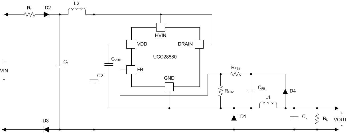 Figure 17. High-Side Buck Converter Schematic
8.2.2.1 Design Requirements
Table 4. 2 Design specification
| DESCRIPTION | MIN | MAX | UNIT | |
|---|---|---|---|---|
| Design Input | ||||
| VIN | AC input Voltage | 85 | 265 | VRMS |
| fLINE | Line frequency | 47 | 63 | Hz |
| IOUT | Output current | 0 | 100 | mA |
| Design requirements | ||||
| PNL | No-load input power | 50 | mW | |
| VOUT | Output voltage | 12 | 14 | V |
| ΔVOUT | Output voltage ripple | 250 | mV | |
| η | Converter efficiency | 68% | ||
8.2.2.2 Detailed Design Procedure
The low-side buck converter and high-side buck converter design procedures are very similar.
8.2.2.2.1 Feedback path (CFB, RFB1 and RFB2) and Load Resistor (RL)
In low-side buck converter the output voltage is always sensed by the FB pin and UCC28880 internal controller can turn on the MOSFET on VOUT. In high-side buck converter applications the information on the output voltage value is stored on CFB capacitor. This information is not updated in real time. The information on CFB capacitor is updated just after MOSFET turn-off event. When the MOSFET is turned off, the inductor current forces the freewheeling diode (D1 in Figure 17) to turn on and the GND pin of UCC28880 goes negative at -Vd1 (where Vd1 is the forward drop voltage of diode D1) with respect to the negative terminal of bulk capacitor (C1 in Figure 17). When D1 is on, through diode D4, the CFB capacitor is charged at VOUT – Vd4 + Vd1. Set the output voltage regulation level using Equation 18.
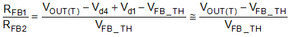
where
- VFB_TH is the FB pin reference voltage.
- VOUT_T is the target output voltage.
- RFB1, RFB2 is the resistance of the resistor divider connected with FB pin (see Figure 17)
- The capacitor CFB after D1 is discharged with a time constant that is τfb = CFB x (RFB1 + RFB2 ).
- Select the time constant τFB, given in Equation 19
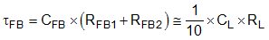
The time constant selection leads to a slight output-voltage increase in no-load or light-load conditions. In order to reduce the output-voltage increase, increase τFB. The drawback of increasing τFB is t in high-load conditions VOUT could drop.
8.2.2.3 Application Curves
Figure 18 shows the output voltage vs output current. Different plots correspond to different converter AC input voltages. Figure 19 shows efficiency changes vs output power. Different plots correspond to different converter AC input voltages.
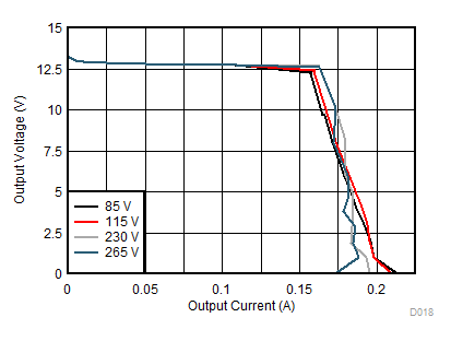 Figure 18. Output IV Characteristic
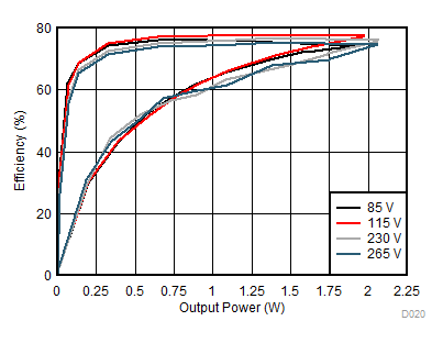 Figure 19. Efficiency vs POUT
Table 5. Converter Efficiency
| VIN_AC (VRMS) | LOAD (mA) | EFFICIENCY (%) | AVERAGE EFFICIENCY (%) |
|---|---|---|---|
| 115 | 25 | 75.2 | 76.8 |
| 50 | 77.1 | ||
| 75 | 77.6 | ||
| 100 | 77.7 | ||
| 230 | 25 | 72.6 | 74.8 |
| 50 | 75.1 | ||
| 75 | 75.7 | ||
| 100 | 76.3 |
Table 6. No-Load and Output Shorted Converter Input Power
| VIN (VRMS) | NO LOAD PIN (mW) | OUTPUT SHORTED PIN (mW) | OUTPUT SHORTED IOUT (mA) |
|---|---|---|---|
| 85 | 31 | 415 | 212 |
| 115 | 34 | 399 | 209 |
| 140 | 36 | 414 | 211 |
| 170 | 38 | 401 | 208 |
| 230 | 44 | 394 | 195 |
| 265 | 47 | 333 | 174 |
8.2.3 Additional UCC28880 Application Topologies
8.2.3.1 Low-Side Buck and LED Driver – Direct Feedback (level-shifted)
Features include:
- Output Referenced to Input
- Negative Output (VOUT) with Respect to VIN+
- Step Down: VOUT < VIN
- Direct Level-Shifted Feedback
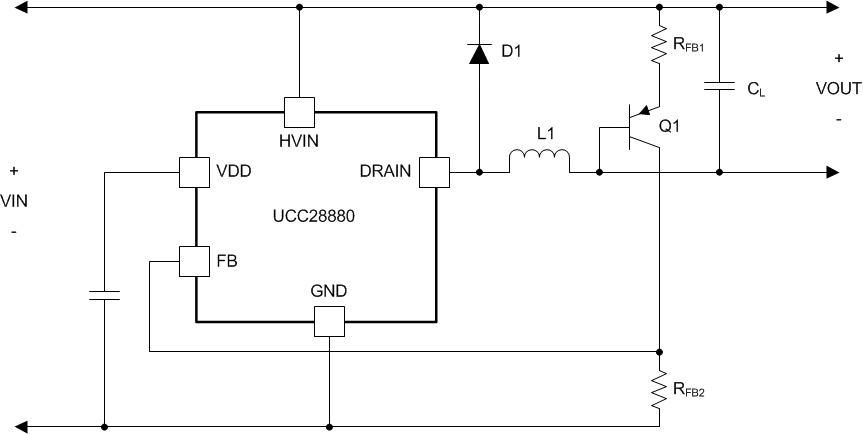 Figure 20. Low-Side Buck – Direct feedback (level-shifted)
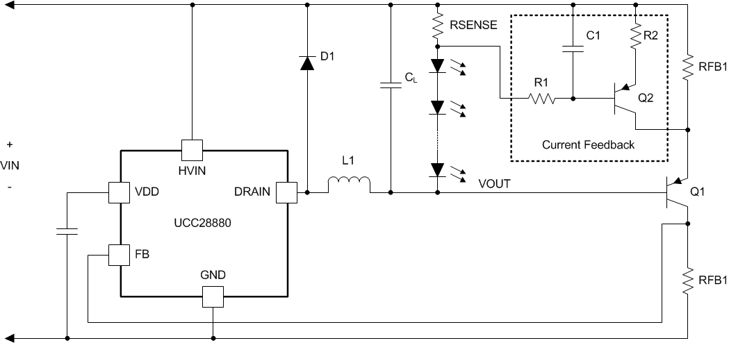 Figure 21. Low-Side Buck LED Driver – Direct feedback (level-shifted)
8.2.3.2 12-V, 100-mA High-Side Buck Converter
Features include:
- Output Referenced to Input
- Positive Output (V ) with Respect to VIN-
- Step Down (VOUT < VIN)
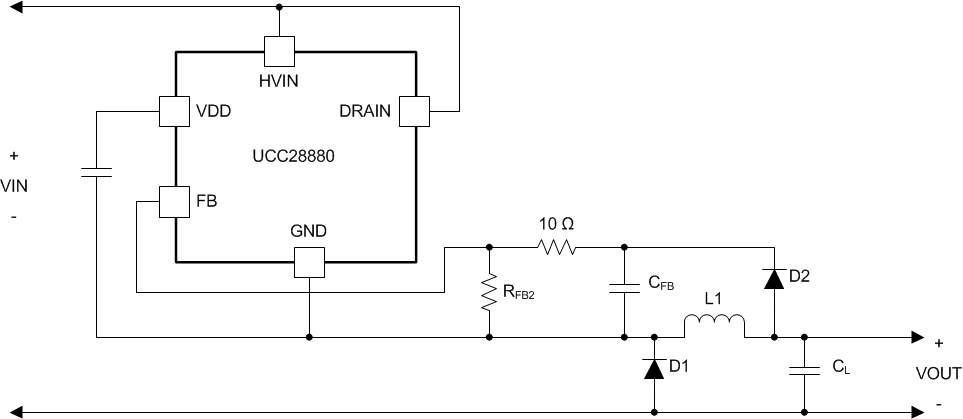 Figure 22. High-Side Buck Converter Schematic
8.2.3.3 Non-Isolated, Low-Side Buck-Boost Converter
Features Include:
- Output referenced to input
- Positive output (VOUT) with respect to VIN+
- Step Up, Step Down: VOUT </> VIN
- Direct Level-Shifted Feedback
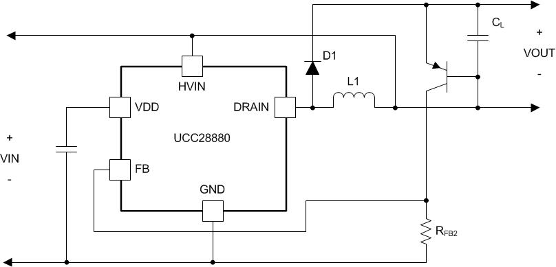 Figure 23. Low-Side Buck-Boost Converter
8.2.3.4 9.5 Non-Isolated, High-Side Buck-Boost Converter
Features include:
- Output Referenced to Input
- Positive Output (VOUT) with Respect to VIN-
- Step Up, Step Down: VOUT </> VIN
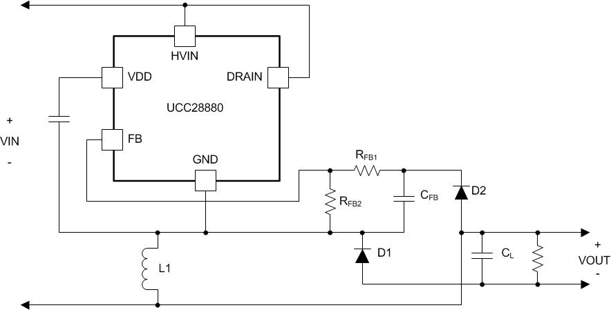 Figure 24. High-Side Buck-Boost Converter
8.2.3.5 9.6 Non-Isolated Flyback Converter
Features include:
- Output Referenced to Input
- Positive Output (VOUT) with Respect VIN-
- Direct Feedback
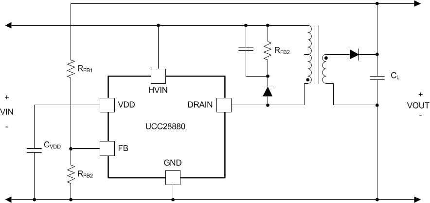 Figure 25. Non-Isolated Flyback Configuration
8.2.3.6 Isolated Flyback Converter
Features include:
- Output Isolated from
- Input Direct Feedback
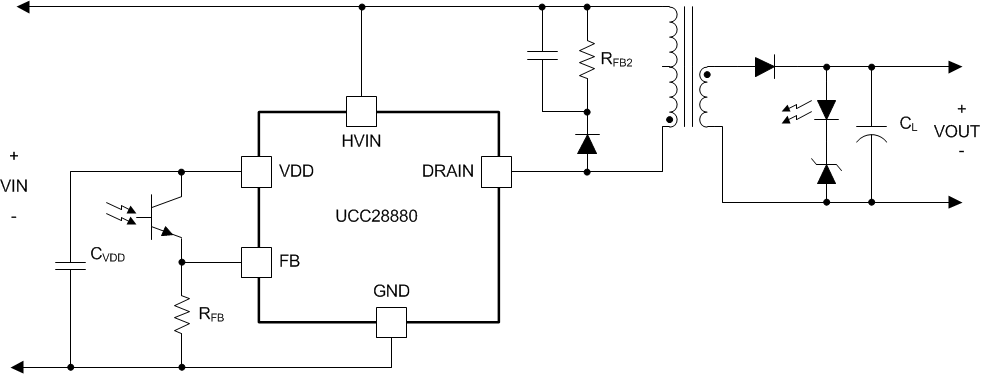 Figure 26. Isolated Flyback Converter