ZHCSCP2 July 2014 UCC28880
PRODUCTION DATA.
- 1 特性
- 2 应用
- 3 说明
- 4 修订历史记录
- 5 Pin Configuration and Functions
- 6 Specifications
- 7 Detailed Description
-
8 Application and Implementation
- 8.1 Application Information
- 8.2
Typical Application
- 8.2.1 12-V, 100-mA Low-Side Buck Converter
- 8.2.2 12-V, 100-mA, High-Side Buck Converter
- 8.2.3
Additional UCC28880 Application Topologies
- 8.2.3.1 Low-Side Buck and LED Driver - Direct Feedback (level-shifted)
- 8.2.3.2 12-V, 100-mA High-Side Buck Converter
- 8.2.3.3 Non-Isolated, Low-Side Buck-Boost Converter
- 8.2.3.4 9.5 Non-Isolated, High-Side Buck-Boost Converter
- 8.2.3.5 9.6 Non-Isolated Flyback Converter
- 8.2.3.6 Isolated Flyback Converter
- 9 Power Supply Recommendations
- 10Layout
- 11器件和文档支持
- 12机械封装和可订购信息
6 Specifications
6.1 Absolute Maximum Ratings
over operating free-air temperature range (unless otherwise noted) (1)(2)| MIN | MAX | UNIT | ||
|---|---|---|---|---|
| HVIN | –0.3 | 700 (3) | V | |
| DRAIN | Internally clamped | 700(3) | V | |
| IDRAIN | Positive drain current single pulse, pulse max duration 25 μs | 320 | mA | |
| IDRAIN | Negative drain current | –320 | mA | |
| FB | –0.3 | 6 | V | |
| VDD | –0.3 | 6 | V |
(1) Stresses beyond those listed under Absolute Maximum Ratings may cause permanent damage to the device. These are stress ratings only, which do not imply functional operation of the device at these or any other conditions beyond those indicated under Recommended Operating Conditions. Exposure to absolute-maximum-rated conditions for extended periods may affect device reliability.
(2) All voltages are with respect to GND. Currents are positive into, negative out of the specified terminal. These ratings apply over the operating ambient temperature ranges unless otherwise noted.
(3) TA = 25°C
6.2 Handling Ratings
| MIN | MAX | UNIT | |||
|---|---|---|---|---|---|
| Tstg | Storage temperature range | –65 | 150 | °C | |
| Lead temperature 1.6 mm (1/16 inch) from case 10 seconds | 260 | ||||
| V(ESD) | Electrostatic discharge | Human Body Model (HBM), per ANSI/ESDA/JEDEC JS-001, all pins(1) | –2000 | 2000 | V |
| Human Body Model (HBM) per ANSI/ESDA/JEDEC JS-001, HVIN pin (1) | –1500 | 1500 | |||
| Charged device model (CDM), per JEDEC specification JESD22-C101, all pins(2) | –500 | 500 | |||
(1) JEDEC document JEP155 states that 500-V HBM allows safe manufacturing with a standard ESD control process.
(2) JEDEC document JEP157 states that 250-V CDM allows safe manufacturing with a standard ESD control process.
6.3 Recommended Operating Conditions
over operating free-air temperature range (unless otherwise noted)| MIN | NOM | MAX | UNIT | ||
|---|---|---|---|---|---|
| VVDD | Voltage On VDD pin | 5 | V | ||
| VFB | Voltage on FB pin | –0.2 | 5 | V | |
| TA | Operating ambient temperature | –40 | 105 | °C | |
| TJ | Operating junction temperature | –40 | 125 | °C | |
6.4 Thermal Information
| THERMAL METRIC(1) | UCC28880 | UNIT | |
|---|---|---|---|
| SOIC (D) | |||
| 7 PINS | |||
| RθJA | Junction-to-ambient thermal resistance | 134.4 | °C/W |
| RθJC(top) | Junction-to-case (top) thermal resistance | 42.6 | |
| RθJB | Junction-to-board thermal resistance | 85 | |
| ψJT | Junction-to-top characterization parameter | 6.4 | |
| ψJB | Junction-to-board characterization parameter | 76 | |
(1) For more information about traditional and new thermal metrics, see the IC Package Thermal Metrics application report, SPRA953.
6.5 Electrical Characteristics
VHVIN = 30 V, TA = TJ = –40°C to 125°C (unless otherwise noted)| PARAMETER | TEST CONDITIONS | MIN | TYP | MAX | UNIT | |
|---|---|---|---|---|---|---|
| VHVIN(min) | Minimum Voltage to startup | 30 | V | |||
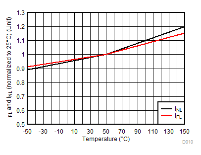
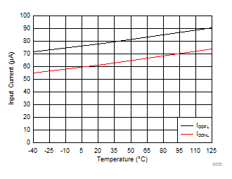
| INL | Internal supply current, no load | FB = 1.25 V (> VFB_TH) | 58 | 100 | µA | |
| IFL | Internal supply current, full load | FB = 0.75 V (> VFB_TH) | 72 | 120 | µA | |
| ICH0 | Charging VDD Cap current | VVDD = 0 V, | –3.8 | –1.6 | –0.4 | mA |
| ICH1 | Charging VDD Cap current | VVDD = 4.4V, VFB = 1.25 V | –3.40 | –1.30 | –0.25 | mA |
| VVDD | Internally regulated low Voltage supply (supplied from HVIN pin) | 4.5 | 5.0 | 5.5 | V | |
| VFB_TH | FB pin reference threshold | 0.94 | 1.02 | 1.10 | V | |
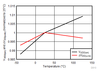
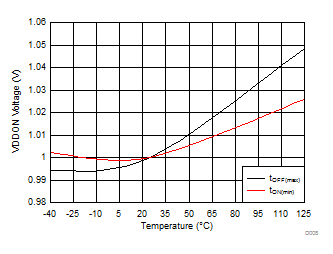
| VVDD(on) | VDD turn-on threshold | VDD low-to-high | 3.55 | 3.92 | 4.28 | V |
| ΔVVDD(uvlo) | VDDON - VDD turn-off threshold | VDD high-to-low | 0.28 | 0.33 | 0.38 | V |
| DMAX | Maximum Duty Cycle | FB = 0.75 V | 45% | 55% | ||
| ILIMIT | Current Limit | Static, TA = –40°C | 300 | mA | ||
| Static, TA = 25°C | 170 | 210 | 260 | mA | ||
| Static, TA = 125°C | 140 | mA | ||||
| TJ(stop) | Thermal Shutdown Temperature | Internal junction temperature | 150 | °C | ||
| TJ(hyst) | Thermal Shutdown Hysteresis | Internal junction temperature | 50 | °C | ||
| BV | Power Mosfet Breakdown Voltage | TJ = 25°C | 700 | °C | ||
| RDS(on) | Power MOSFET On-Resistance (includes internal sense-resistor) | ID = 30 mA, TJ = 25°C | 32 | 40 | Ω | |
| ID = 30 mA, TJ = 125°C | 55 | 68 | Ω | |||
| DRAIN_ILEAKAGE | Power MOSFET off state leakage current | VDRAIN = 700V, TJ = 25°C | 5 | µA | ||
| VDRAIN = 400 V, TJ = 125°C | 20 | µA | ||||
| HVIN_IOFF | HVIN off state current | VHVIN = 700 V, TJ = 25°C, VVDD = 5.8 V | 4.0 | 7.5 | 12.0 | µA |
| VHVIN = 400 V, TJ = 125°C, VVDD = 5.8 V | 20 | µA | ||||
6.6 Switching Characteristics
over operating free-air temperature range (unless otherwise noted)| PARAMETER | TEST CONDITIONS | MIN | TYP | MAX | UNIT | |
|---|---|---|---|---|---|---|
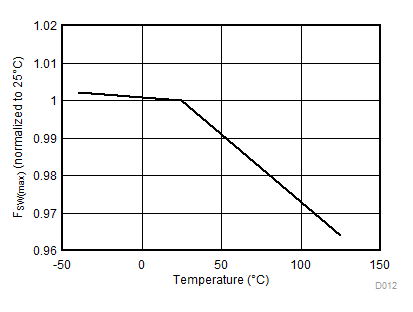
| fSW(max) | Maximum switching frequency | 52 | 62 | 75 | kHz | |
| tON_MAX | Maximum switch on time (current limiter not triggered), | FB = 0.75 V | 5.7 | 7.6 | 9.5 | µs |
| tOFF_MIN | Minimum switch off time follows every tON time, | FB = 0.75 V | 5.7 | 7.6 | 9.5 | µs |
| tMIN | Minimum on time | 0.17 | 0.22 | 0.30 | µs | |
| tOFF(ovl) | Max off time (OL condition), tOFF(ovl) = tSW – tON(max) | 130 | 200 | 270 | µs | |
6.7 Typical Characteristics
A.
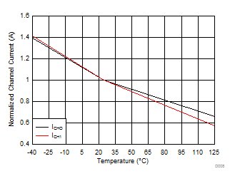
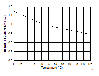
Figure 1. ILIMIT vs Temperature
A.
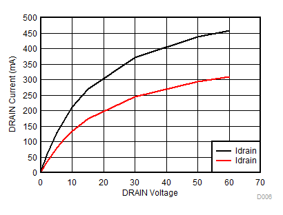
Figure 2. ILIMIT vs Drain Current Slope