ZHCSCP2 July 2014 UCC28880
PRODUCTION DATA.
- 1 特性
- 2 应用
- 3 说明
- 4 修订历史记录
- 5 Pin Configuration and Functions
- 6 Specifications
- 7 Detailed Description
-
8 Application and Implementation
- 8.1 Application Information
- 8.2
Typical Application
- 8.2.1 12-V, 100-mA Low-Side Buck Converter
- 8.2.2 12-V, 100-mA, High-Side Buck Converter
- 8.2.3
Additional UCC28880 Application Topologies
- 8.2.3.1 Low-Side Buck and LED Driver - Direct Feedback (level-shifted)
- 8.2.3.2 12-V, 100-mA High-Side Buck Converter
- 8.2.3.3 Non-Isolated, Low-Side Buck-Boost Converter
- 8.2.3.4 9.5 Non-Isolated, High-Side Buck-Boost Converter
- 8.2.3.5 9.6 Non-Isolated Flyback Converter
- 8.2.3.6 Isolated Flyback Converter
- 9 Power Supply Recommendations
- 10Layout
- 11器件和文档支持
- 12机械封装和可订购信息
5 Pin Configuration and Functions
Top View
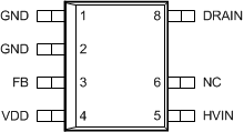
Pin Functions
| PIN | I/O | DESCRIPTION | |
|---|---|---|---|
| NAME | NO. | ||
| GND | 1 | G | Ground |
| GND | 2 | G | Ground |
| FB | 3 | I | Feedback terminal |
| VDD | 4 | O | Supply pin, supply is provided by internal LDO |
| HVIN | 5 | P | Supply pin |
| NC | 6 | N/C | Not internally connected |
| DRAIN | 8 | P | Drain pin |