ZHCSGD9 June 2017 UCC28730-Q1
PRODUCTION DATA.
- 1 特性
- 2 应用
- 3 说明
- 4 修订历史记录
- 5 Pin Configuration and Functions
- 6 Specifications
-
7 Detailed Description
- 7.1 Overview
- 7.2 Functional Block Diagram
- 7.3 Feature Description
- 7.4 Device Functional Modes
-
8 Application and Implementation
- 8.1 Application Information
- 8.2
Typical Application
- 8.2.1 Design Requirements
- 8.2.2
Detailed Design Procedure
- 8.2.2.1 Stand-By Power Estimate
- 8.2.2.2 Input Bulk Capacitance and Minimum Bulk Voltage
- 8.2.2.3 Transformer Turns Ratio, Inductance, Primary-Peak Current
- 8.2.2.4 Transformer Parameter Verification
- 8.2.2.5 Output Capacitance
- 8.2.2.6 VDD Capacitance, CVDD
- 8.2.2.7 VS Resistor Divider, Line Compensation, and Cable Compensation
- 8.2.2.8 VS Wake-Up Detection
- 8.2.3 Application Curves
- 8.3 Do's and Don'ts
- 9 Power Supply Recommendations
- 10Layout
- 11器件和文档支持
- 12机械、封装和可订购信息
6 Specifications
6.1 Absolute Maximum Ratings
over operating free-air temperature range (unless otherwise noted)(1)| MIN | MAX | UNIT | ||
|---|---|---|---|---|
| Voltage | HV | 700 | V | |
| VDD | 38 | V | ||
| VS | –0.75 | 7 | V | |
| CS, CBC | –0.5 | 5 | V | |
| DRV | –0.5 | Self-limiting | V | |
| Current | DRV, continuous sink | 50 | mA | |
| DRV, source | Self-limiting | mA | ||
| VS, peak, 1% duty-cycle | –1.2 | mA | ||
| Lead temperature 0.6 mm from case for 10 seconds | –65 | 150 | °C | |
| Storage temperature, Tstg | 260 | °C | ||
(1) Stresses beyond those listed under Absolute Maximum Ratings may cause permanent damage to the device. These are stress ratings only, which do not imply functional operation of the device at these or any other conditions beyond those indicated under Recommended Operating Conditions. Exposure to absolute-maximum-rated conditions for extended periods may affect device reliability.
6.2 ESD Ratings
| VALUE | UNIT | |||
|---|---|---|---|---|
| V(ESD) | Electrostatic discharge | Human-body model (HBM), per AEC Q100-002(1) | ±2000 | V |
| Charged-device model (CDM), per AEC Q100-011 | ±750 | |||
(1) AEC Q100-002 indicates that HBM stressing shall be in accordance with the ANSI/ESDA/JEDEC JS-001 specification.
6.3 Recommended Operating Conditions
over operating free-air temperature range (unless otherwise noted)| MIN | NOM | MAX | UNIT | ||
|---|---|---|---|---|---|
| VVDD | Bias-supply operating voltage | 9 | 35 | V | |
| CVDD | VDD by-pass capacitor | 0.047 | µF | ||
| RCBC | Cable-compensation resistance | 10 | kΩ | ||
| IVS | VS pin current, out of pin | 1 | mA | ||
| TJ | Operating junction temperature | –40 | 125 | °C | |
6.4 Thermal Information
| THERMAL METRIC(1) | UCC28730-Q1 | UNIT | |
|---|---|---|---|
| D (SOIC) | |||
| 7 PINS | |||
| RθJA | Junction-to-ambient thermal resistance | 128.0 | °C/W |
| RθJC(top) | Junction-to-case (top) thermal resistance | 59.3 | °C/W |
| RθJB | Junction-to-board thermal resistance | 66.7 | °C/W |
| ψJT | Junction-to-top characterization parameter | 17.0 | °C/W |
| ψJB | Junction-to-board characterization parameter | 65.9 | °C/W |
(1) For more information about traditional and new thermal metrics, see the Semiconductor and IC Package Thermal Metrics application report.
6.5 Electrical Characteristics
over operating free-air temperature range, VVDD = 25 V, HV = open, RCBC = open, TA = -40°C to 125°C (unless otherwise noted)| PARAMETER | TEST CONDITION | MIN | TYP | MAX | UNIT | |
|---|---|---|---|---|---|---|
| HIGH-VOLTAGE START-UP | ||||||
| IHV | Start-up current out of VDD | VHV = 100 V, VVDD = 0 V, start state | 100 | 250 | 500 | µA |
| IHVLKG25 | Leakage current into HV | VHV = 400 V, run state, TJ = 25°C | 0.01 | 0.5 | µA | |
| BIAS SUPPLY INPUT CURRENT | ||||||
| IRUN | Supply current, run | Run state, IDRV = 0 A | 2.1 | 2.65 | mA | |
| IWAIT | Supply current, wait | Wait state, IDRV = 0 A, VVDD = 20 V | 52 | 75 | µA | |
| ISTART | Supply current, start | Start state, IDRV = 0 A, VVDD = 18 V, IHV = 0 A | 18 | 30 | µA | |
| IFAULT | Supply current, fault | Fault state, IDRV = 0 A | 54 | 75 | µA | |
| UNDER-VOLTAGE LOCKOUT | ||||||
| VVDD(on) | VDD turn-on threshold | VVDD low to high | 17.5 | 21 | 23 | V |
| VVDD(off) | VDD turn-off threshold | VVDD high to low | 7.3 | 7.7 | 8.1 | V |
| VS Input and Wake-Up Monitor | ||||||
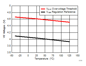
| VVSR | Regulating level(1) | Measured at no-load condition, TJ = 25°C | 4.00 | 4.04 | 4.08 | V(1) |
| VVSNC | Negative clamp level below GND | IVSLS = –300 µA | 190 | 250 | 325 | mV |
| IVSB | Input bias current | VVS = 4 V | –0.25 | 0 | 0.25 | µA |
| VWU(high) | Wake-up threshold at VS, high(2) | VS pin rising | 2 | V(2) | ||
| VWU(low) | Wake-up threshold at VS, low | VS pin rising | 15 | 57 | 105 | mV |
| CS INPUT | ||||||
| VCST(max) | CS maximum threshold voltage(3) | VVS = 3.7 V | 710 | 740 | 770 | mV(3) |
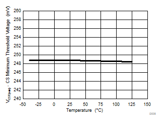
| VCST(min) | CS minimum threshold voltage | VVS = 4.35 V | 230 | 249 | 270 | mV |
| KAM | AM control ratio, VCST(max) / VCST(min) | 2.75 | 2.99 | 3.20 | V/V | |
| VCCR | Constant-current regulation factor | 310 | 319 | 329 | mV | |
| KLC | Line compensation current ratio, IVSLS / current out of CS pin | IVSLS = –300 µA | 24 | 25.3 | 28 | A/A |
| DRIVER | ||||||
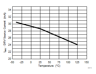
| IDRS | DRV source current | VDRV = 8 V, VVDD = 9 V | 20 | 29 | 35 | mA |
| RDRVLS | DRV low-side drive resistance | IDRV = 10 mA | 6 | 12 | Ω | |
| VDRCL | DRV clamp voltage | VVDD = 35 V | 13 | 14.5 | 16 | V |
| RDRVSS | DRV pull-down in start state | 150 | 190 | 230 | kΩ | |
| PROTECTION | ||||||
| VOVP | Over-voltage threshold(1) | At VS input, TJ = 25°C | 4.52 | 4.62 | 4.71 | V(1) |
| VOCP | Over-current threshold | At CS input | 1.4 | 1.5 | 1.6 | V |
| IVSL(run) | VS line-sense run current | Current out of VS pin increasing | 190 | 225 | 275 | µA |
| IVSL(stop) | VS line-sense stop current | Current out of VS pin decreasing | 70 | 80 | 100 | µA |
| KVSL | VS line-sense ratio, IVSL(run) / IVSL(stop) | 2.45 | 2.8 | 3.05 | A/A | |
| TJ(stop) | Thermal shut-down temperature | Internal junction temperature | 165 | °C | ||
| CABLE COMPENSATION | ||||||
| VCBC(max) | Cable compensation output maximum voltage | Voltage at CBC at full load | 2.9 | 3.13 | 3.5 | V |
| VCVS(min) | Minimum compensation at VS | VCBC = open, change in VS regulating level from no load to full load | –50 | –15 | 20 | mV |
| VCVS(max) | Maximum compensation at VS | VCBC = 0 V, change in VS regulating level from no load to full load | 275 | 325 | 375 | mV |
(1) The regulating level and OV threshold at VS decrease with increasing temperature by 1 mV/°C. This compensation over temperature is included to reduce the variances in power supply output regulation and over-voltage detection with respect to the external output rectifier.
(2) Designed for accuracy within ±10% of typical value.
(3) These threshold voltages represent average levels. This device automatically varies the current sense thresholds to improve EMI performance.
6.6 Timing Requirements
| MIN | NOM | MAX | UNIT | ||
|---|---|---|---|---|---|
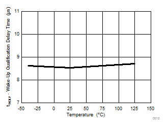
| tWUDLY | Wake-up qualification delay, VVS = 0 V | 7.0 | 8.5 | 11.0 | µs |
| tCSLEB | Leading-edge blanking time , DRV output duration, VCS = 1 V | 170 | 225 | 280 | ns |
| tZTO | Zero-crossing timeout delay, no zero-crossing detected | 1.6 | 2.2 | 2.9 | µs |
6.7 Switching Characteristics
over operating free-air temperature range (unless otherwise noted)| PARAMETER | TEST CONDITIONS | MIN | TYP | MAX | UNIT | |
|---|---|---|---|---|---|---|
| fSW(max) | Maximum switching frequency(1) | VVS = 3.7 V | 76.0 | 83.3 | 90.0 | kHz |
| fSW(min) | Minimum switching frequency | VVS = 4.35 V | 25 | 32 | 37 | Hz |
(1) These frequency limits represent average levels. This device automatically varies the switching frequency to improve EMI performance.
6.8 Typical Characteristics
VVDD = 25 V, TJ = 25°C, unless otherwise noted.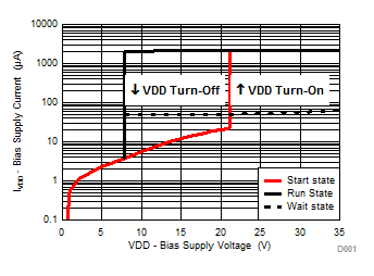
| IHV = 0 A | IDRV = 0 A |
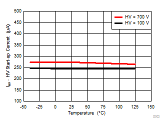
| VVDD = 0 V |
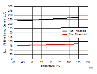
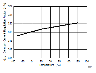
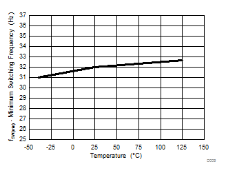
| VVS = 4.35 V |
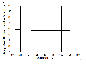
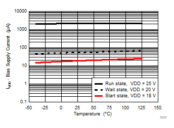
| IHV = 0 A | IDRV = 0 A |
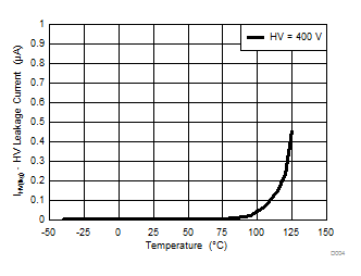
| VVDD = 25 V |
| VVDD = 9 V | VDRV = 8 V |
| VVS = 0 V |