ZHCSKO8C June 2021 – January 2022 UCC27614
PRODUCTION DATA
- 1 特性
- 2 应用
- 3 说明
- 4 Revision History
- 5 Pin Configuration and Functions
- 6 Specifications
- 7 Detailed Description
- 8 Applications and Implementation
- 9 Power Supply Recommendations
- 10Layout
- 11Device and Documentation Support
- 12Mechanical, Packaging, and Orderable Information
封装选项
机械数据 (封装 | 引脚)
散热焊盘机械数据 (封装 | 引脚)
- DSG|8
订购信息
8.2.1.2.7 Power Dissipation
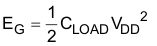
Power dissipation of the gate driver has two portions as shown in equation below:

The DC portion of the power dissipation is PDC = IQ × VDD where IQ is the quiescent current for the driver. The quiescent current is the current consumed by the device to bias all internal circuits such as input stage, reference voltage, logic circuits, protections, and so on, and any current associated with switching of internal devices when the driver output changes state (such as charging and discharging of internal parasitic capacitances, parasitic shoot-through). The UCC27614 features low quiescent currents (less than 1 mA) and contains internal logic to minimize any shoot-through (PMOS to NMOS and vice versa) in the output driver stage. Thus, the effect of the PDC on the total power dissipation within the gate driver can be assumed to be negligible. In practice this is the power consumed by driver when its output is disconnected from the gate of power switch.
As explained in earlier sections, the output stage of the gate driver is based on PMOS and NMOS. These NMOS and PMOS are designed in such a way that they offer very low resistance during switching. And therefore they have very low drop-out. The power dissipated in the gate driver package during switching (PSW) depends on the following factors:
- Gate charge required of the power device (usually a function of the drive voltage VG, which is very close to input bias supply voltage VDD due to low VOx drop-out)
- Switching frequency
- Power MOSFET internal and external gate resistor
where
- CLOAD is load capacitor and VDD is bias voltage feeding the driver.
There is an equal amount of energy dissipated when the capacitor is discharged. During turnoff the energy stored in capacitor is fully dissipated in drive circuit. This leads to a total power loss during switching cycle given by the following:
where
- ƒSW is the switching frequency
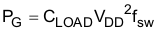
The switching load presented by a power FET and IGBT can be converted to an equivalent capacitance by examining the gate charge required to switch the device. This gate charge includes the effects of the input capacitance plus the added charge needed to swing the drain voltage of the power device as it switches between the ON and OFF states. Most manufacturers provide specifications of typical and maximum gate charge, in nC, to switch the device under specified conditions. Using the gate charge Qg, one can determine the power that must be dissipated when charging a capacitor. This is done by using the equivalence, Qg = CLOADVDD, to provide the following equation for power:
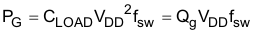
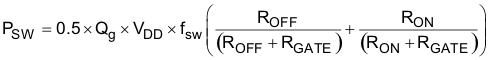
This power PG is dissipated in the resistive elements of the circuit when the MOSFET and IGBT is being turned on or off. Half of the total power is dissipated when the load capacitor is charged during turnon, and the other half is dissipated when the load capacitor is discharged during turn-off. When no external gate resistor is employed between the driver IC and MOSFET/IGBT, this power is completely dissipated inside the driver IC. With the use of external gate drive resistors, the power dissipation is shared between the internal resistance of driver and external gate resistor in accordance to the ratio of the resistances (more power dissipated in the higher resistance component). Based on this simplified analysis, the driver power dissipation during switching is calculated as shown in following equation. This primarily applies to those applications where total external gate resistor is significantly large to limit the peak current of the gate driver.
where
- ROFF = ROL and RON (effective resistance of pullup structure)