ZHCSK29B september   2019  – october 2020 UCC23511

PRODUCTION DATA  

  1.   1
  2. 特性
  3. 应用
  4. 说明
  5. Revision History
  6. Pin Configuration and Function
    1.     Pin Functions
  7. Specifications
    1. 6.1  Absolute Maximum Ratings
    2. 6.2  ESD Ratings
    3. 6.3  Recommended Operating Conditions
    4. 6.4  Thermal Information
    5. 6.5  Power Ratings
    6. 6.6  Insulation Specifications
    7. 6.7  Safety-Related Certifications
    8. 6.8  Safety Limiting Values
    9. 6.9  Electrical Characteristics
    10. 6.10 Switching Characteristics
    11. 6.11 Insulation Characteristics Curves
    12. 6.12 Typical Characteristics
  8. Parameter Measurement Information
    1. 7.1 Propagation Delay, rise time and fall time
    2. 7.2 IOH and IOL testing
    3. 7.3 CMTI Testing
  9. Detailed Description
    1. 8.1 Overview
    2. 8.2 Functional Block Diagram
    3. 8.3 Feature Description
      1. 8.3.1 Power Supply
      2. 8.3.2 Input Stage
      3. 8.3.3 Output Stage
      4. 8.3.4 Protection Features
        1. 8.3.4.1 Undervoltage Lockout (UVLO)
        2. 8.3.4.2 Active Pulldown
        3. 8.3.4.3 Short-Circuit Clamping
    4. 8.4 Device Functional Modes
      1. 8.4.1 ESD Structure
  10. Application and Implementation
    1. 9.1 Application Information
    2. 9.2 Typical Application
      1. 9.2.1 Design Requirements
      2. 9.2.2 Detailed Design Procedure
        1. 9.2.2.1 Selecting the Input Resistor
        2. 9.2.2.2 Gate Driver Output Resistor
        3. 9.2.2.3 Estimate Gate-Driver Power Loss
        4. 9.2.2.4 Estimating Junction Temperature
        5. 9.2.2.5 Selecting VCC Capacitor
  11. 10Power Supply Recommendations
  12. 11Layout
    1. 11.1 Layout Guidelines
    2. 11.2 Layout Example
    3. 11.3 PCB Material
    4. 11.4 Custom Design With WEBENCH® Tools
  13. 12Mechanical, Packaging, and Orderable Information

封装选项

请参考 PDF 数据表获取器件具体的封装图。

机械数据 (封装 | 引脚)
  • DWY|6
散热焊盘机械数据 (封装 | 引脚)
订购信息

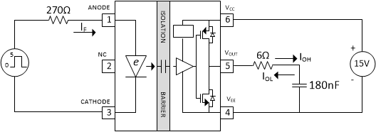
IOH and IOL testing

Figure 7-2 shows the circuit used to measure the output drive currents IOH and IOL. A series resistor of 6 Ω and a load capacitance of 180 nF are used at the output. The peak dv/dt of the capacitor voltage is measured in order to determine the peak source and sink currents of the gate driver.
GUID-FBCBED02-0CCF-43E4-9E77-437061BB42B3-low.gifFigure 7-2 IOH and IOL