ZHCSKC0 October 2019 UCC21736-Q1
ADVANCE INFORMATION for pre-production products; subject to change without notice.
- 1 特性
- 2 应用
- 3 说明
- 4 修订历史记录
- 5 Pin Configuration and Functions
-
6 Specifications
- 6.1 Absolute Maximum Ratings
- 6.2 ESD Ratings
- 6.3 Recommended Operating Conditions
- 6.4 Thermal Information
- 6.5 Power Ratings
- 6.6 Electrical Characteristics
- 6.7 Switching Characteristics
- 6.8 Insulation Specifications
- 6.9 Safety-Related Certifications
- 6.10 Safety Limiting Values
- 6.11 Insulation Characteristics Curves
- 6.12 Typical Characteristics
- 7 Parameter Measurement Information
-
8 Detailed Description
- 8.1 Overview
- 8.2 Functional Block Diagram
- 8.3
Feature Description
- 8.3.1 Power Supply
- 8.3.2 Driver Stage
- 8.3.3 VCC, VDD and VEE Undervoltage Lockout (UVLO)
- 8.3.4 Active Pulldown
- 8.3.5 Short Circuit Clamping
- 8.3.6 External Active Miller Clamp
- 8.3.7 Overcurrent and Short Circuit Protection
- 8.3.8 Fault (FLT, Reset and Enable (RST/EN)
- 8.3.9 ASC Protection and APWM Monitor
- 8.4 Device Functional Modes
-
9 Applications and Implementation
- 9.1 Application Information
- 9.2
Typical Application
- 9.2.1 Design Requirements
- 9.2.2
Detailed Design Procedure
- 9.2.2.1 Input filters for IN+, IN- and RST/EN
- 9.2.2.2 PWM Interlock of IN+ and IN-
- 9.2.2.3 FLT, RDY and RST/EN Pin Circuitry
- 9.2.2.4 RST/EN Pin Control
- 9.2.2.5 Turn on and turn off gate resistors
- 9.2.2.6 External Active Miller Clamp
- 9.2.2.7 Overcurrent and Short Circuit Protection
- 9.2.2.8 Higher Output Current Using an External Current Buffer
- 10Power Supply Recommendations
- 11Layout
- 12器件和文档支持
- 13机械、封装和可订购信息
6.12 Typical Characteristics
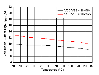 Figure 4. Output High Drive Current vs. Temperature
 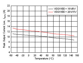 Figure 5. Output Low Driver Current vs. Temperature
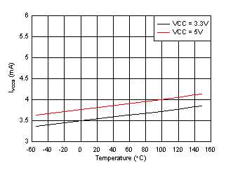
1.
Figure 6. IVCCQ Supply Current vs. Temperature | IN+ = High | IN- = Low |
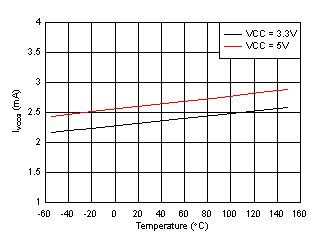
1.
Figure 7. IVCCQ Supply Current vs. Temperature | IN+ = Low | IN- = Low |
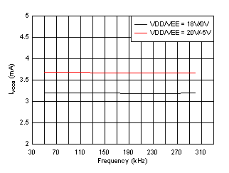 Figure 8. IVCCQ Supply Current vs. Input Frequency
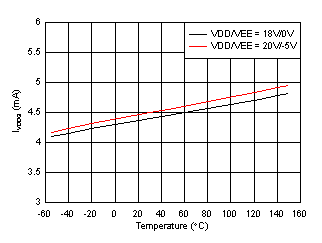
1.
Figure 9. IVDDQ Supply Current vs. Temperature | IN+ = High | IN- = Low |
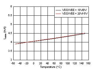
1.
Figure 10. IVDDQ Supply Current vs. Temperature | IN+ = Low | IN- = Low |
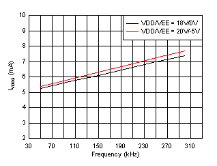
1.
Figure 11. IVDDQ Supply Current vs. Input Frequency 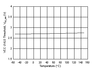 Figure 12. VCC UVLO vs. Temperature
 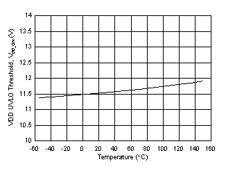 Figure 13. VDD UVLO vs. Temperature
1.
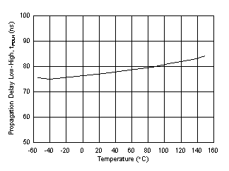
Figure 14. Propagation Delay tPDLH vs. Temperature | VCC = 3.3V | VDD=18V | CL = 100pF |
| RON = 0Ω | ROFF = 0Ω |
1.
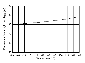
Figure 15. Propagation Delay tPDHL vs. Temperature | VCC = 3.3V | VDD=18V | CL = 100pF |
| RON = 0Ω | ROFF = 0Ω |
1.
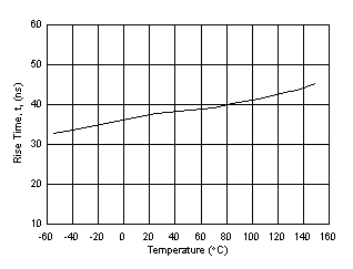
Figure 16. tr Rise Time vs. Temperature | VCC = 3.3V | VDD=18V | CL = 10nF |
| RON = 0Ω | ROFF = 0Ω |
1.
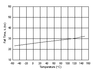
Figure 17. tf Fall Time vs. Temperature | VCC = 3.3V | VDD=18V | CL = 10nF |
| RON = 0Ω | ROFF = 0Ω |
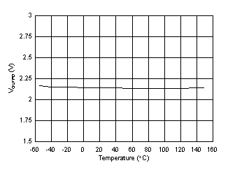 Figure 18. VOUTPD Output Active Pulldown Voltage vs. Temperature
1.
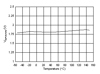
Figure 19. VCLP-OUT(H) Short Circuit Clamping Voltage vs. Temperature 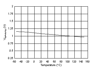
1.
Figure 20. VCLP-OUT(L) Short Circuit Clamping Voltage vs. Temperature 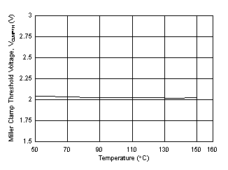 Figure 21. VCLMPTH Miller Clamp Threshold Voltage vs. Temperature
1.
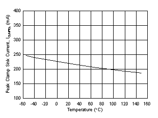
Figure 22. ICLMPEL Miller Clamp Sink Current vs. Temperature 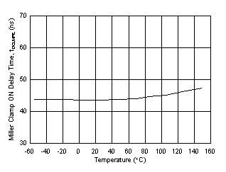
1.
Figure 23. tDCLMPE Miller Clamp ON Delay Time vs. Temperature 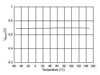
1.
Figure 24. VOCTH OC Detection Threshold vs. Temperature