ZHCS910B November 2011 – April 2016 TXS0206A
PRODUCTION DATA.
- 1 特性
- 2 应用范围
- 3 说明
- 4 修订历史记录
- 5 Pin Configuration and Functions
-
6 Specifications
- 6.1 Absolute Maximum Ratings
- 6.2 ESD Ratings
- 6.3 Recommended Operating Conditions
- 6.4 Thermal Information
- 6.5 Electrical Characteristics
- 6.6 Timing Requirements—VCCA = 1.2 V ± 0.1 V
- 6.7 Timing Requirements—VCCA = 1.8 V ± 0.15 V
- 6.8 Timing Requirements—VCCA = 3.3 V ± 0.3 V
- 6.9 Switching Characteristics—VCCA = 1.2 V ± 0.1 V
- 6.10 Switching Characteristics—VCCA = 1.8 V ± 0.15 V
- 6.11 Switching Characteristics—VCCA = 3.3 V ± 0.3 V
- 6.12 Operating Characteristics —VCCA = 1.2 V
- 6.13 Operating Characteristics —VCCA = 1.8 V
- 6.14 Operating Characteristics — VCCA = 3.3 V
- 6.15 Typical Characteristics
- 7 Parameter Measurement Information
- 8 Detailed Description
- 9 Application and Implementation
- 10Power Supply Recommendations
- 11Layout
- 12器件和文档支持
- 13机械、封装和可订购信息
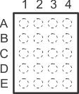
5 Pin Configuration and Functions
YFP Package
20–Pin DSBGA
Top View

Pin Assignments
| 1 | 2 | 3 | 4 | |
|---|---|---|---|---|
| A | DAT2A | VCCA | WP | DAT2B |
| B | DAT3A | CD | VCCB | DAT3B |
| C | CMDA | GND | GND | CMDB |
| D | DAT0A | CLKA | CLKB | DAT0B |
| E | DAT1A | CLK-f | EN | DAT1B |
Pin Functions
| PIN | TYPE | DESCRIPTION | |
|---|---|---|---|
| NO. | NAME | ||
| A1 | DAT2A | I/O | Data bit 2 connected to host. Referenced to VCCA. Includes a 40-kΩ pullup resistor to VCCA. |
| A2 | VCCA | Pwr | A-port supply voltage. VCCA powers all A-port I/Os and control inputs. |
| A3 | WP | O | Connected to write protect on the mechanical connector. The WP pin has an internal 100-kΩ (± 30%) pullup resistor to VCCA. Leave unconnected if not used. |
| A4 | DAT2B | I/O | Data bit 2 connected to memory card. Referenced to VCCB. Includes a 40-kΩ pullup resistor to VCCB. |
| B1 | DAT3A | I/O | Data bit 3 connected to host. Referenced to VCCA. Includes a 40-kΩ pullup resistor to VCCA. |
| B2 | CD | O | Connected to card detect on the mechanical connector. The CD pin has an internal 100-kΩ (± 30%) pullup resistor to VCCA. Leave unconnected if not used. |
| B3 | VCCB | Pwr | B-port supply voltage. VCCB powers all B-port I/Os. |
| B4 | DAT3B | I/O | Data bit 3 connected to memory card. Referenced to VCCB. Includes a 40-kΩ pullup resistor to VCCB. |
| C1 | CMDA | I/O | Command bit connected to host. Referenced to VCCA. Includes a 40-kΩ pullup resistor to VCCA. |
| C2 | GND | — | Ground |
| C3 | GND | — | Ground |
| C4 | CMDB | I/O | Command bit connected to memory card. Referenced to VCCB. Includes a 40-kΩ pullup resistor to VCCB. |
| D1 | DAT0A | I/O | Data bit 0 connected to host. Referenced to VCCA. Includes a 40-kΩ pullup resistor to VCCA. |
| D2 | CLKA | I | Clock signal connected to host. Referenced to VCCA. |
| D3 | CLKB | O | Clock signal connected to memory card. Referenced to VCCB. |
| D4 | DAT0B | I/O | Data bit 0 connected to memory card. Referenced to VCCB. Includes a 40-kΩ pullup resistor to VCCB. |
| E1 | DAT1A | I/O | Data bit 1 connected to host. Referenced to VCCA. Includes a 40-kΩ pullup resistor to VCCA. |
| E2 | CLK-f | O | Clock feedback to host for resynchronizing data to a processor. Leave unconnected if not used. |
| E3 | EN | I | Enable/disable control. Pull EN low to place all outputs in Hi-Z state. Referenced to VCCA. |
| E4 | DAT1B | I/O | Data bit 1 connected to memory card. Referenced to VCCB. Includes a 40-kΩ pullup resistor to VCCB. |