ZHCSCV1A June 2014 – July 2014 TSC2013-Q1
PRODUCTION DATA.
- 1 特性
- 2 应用
- 3 说明
- 4 修订历史记录
- 5 Pin Configurations and Functions
-
6 Specifications
- 6.1 Absolute Maximum Ratings
- 6.2 Handling Ratings
- 6.3 Recommended Operating Conditions
- 6.4 Thermal Information
- 6.5 Electrical Characteristics
- 6.6 Timing Requirements — I2C Standard Mode (ƒ(SCL) = 100 kHz)
- 6.7 Timing Requirements — I2C Fast Mode (ƒ(SCL) = 400 kHz)
- 6.8 Timing Requirements — I2C High-Speed Mode (ƒ(SCL) = 1.7 MHz)
- 6.9 Timing Requirements — I2C High-Speed Mode (ƒ(SCL) = 3.4 MHz)
- 6.10 Typical Characteristics
-
7 Detailed Description
- 7.1 Overview
- 7.2 Functional Block Diagram
- 7.3 Feature Description
- 7.4 Device Functional Modes
- 7.5 Programming
- 7.6
Register Maps
- 7.6.1 Configuration and Status Registers
- 7.6.2 Data Registers
-
8 Application and Implementation
- 8.1 Application Information
- 8.2
Typical Application
- 8.2.1 Design Requirements
- 8.2.2 Detailed Design Procedure
- 8.2.3 Application Curves
- 9 Power Supply Recommendations
- 10Layout
- 11器件和文档支持
- 12机械封装和可订购信息
封装选项
机械数据 (封装 | 引脚)
散热焊盘机械数据 (封装 | 引脚)
- RSA|16
订购信息
8 Application and Implementation
8.1 Application Information
8.1.1 Auxiliary Measurement
The TSC2013-Q1 device can measure the voltage from the auxiliary input (AUX). Applications for the AUX can include external temperature sensing, ambient light monitoring for controlling backlighting, or sensing the current drawn from batteries. Two converter functions can be used for the measurement of the AUX:
- Non-continuous AUX measurement as shown in Figure 44 (converter function select bits C[3:0] = control byte 1 D[6:3] = 0101)
- Continuous AUX measurement as shown in Figure 45 (converter function select bits C[3:0] = control byte 1 D[6:3] = 1000)
See Table 7 for more information on the converter function select bits.
Use Equation 9 to calculate the time required to make a non-continuous auxiliary measurement.
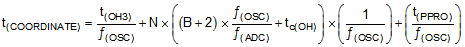
where
- t(OH3) = overhead time number 3 = 3.5 internal clock cycles.
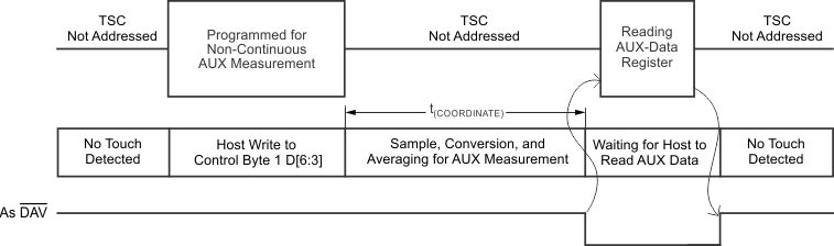 Figure 44. Non-Touch Screen, Non-Continuous AUX Measurement
Use Equation 9 to calculate the time required to make a continuous auxiliary measurement.
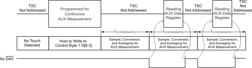 Figure 45. Non-Touch Screen, Continuous AUX Measurement
8.1.2 Single IX or Single IY Measurement
Figure 46 shows the sequence for a single IX or single IY measurement.
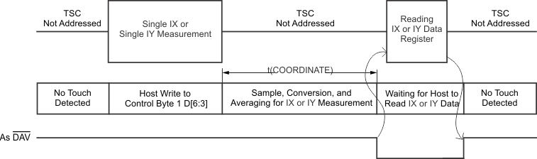 Figure 46. Touch Screen, Single IX or IY Measurement
8.2 Typical Application
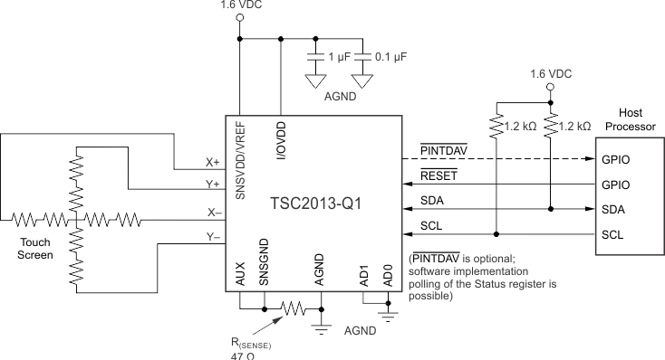 Figure 47. Typical Application Diagram
8.2.1 Design Requirements
The system-level requirements for this design include:
- Normal 4-wire resistive touch screen with low activation force (from center area down to 0.1 to 0.3 N) to enable smooth dual-touch operation.
- The R(SENSE) resistor value is the lowest panel resistance (X or Y layer) which is approximately 4.5. This resistor value provides the best dynamic range for dual-touch separation.
- To achieve the best possible SNR, select the highest operating voltage of the TSC2013-Q1 device that is compatible with the system.
8.2.2 Detailed Design Procedure
Resistive dual touch using TSC2013-Q1 device is based on the principle of measuring resistance changes between X and Y panel. The resistive touch screen has two ITO layers which are located apart from each other. When the user uses a single-finger touch, only a minor parallel connection occurs between these two layers.
During a dual-finger touch when the finger touches are located on different areas of the screen, parallel connection is much higher which results in a reduction in panel resistance. Because the TSC2013-Q1 device measures both X and Y-layer panel resistance, the finger touch distance can be easily calculated from the resistance change. This calculation is achieved by using one external resistor the is connected internally in series with the measured X-Y panel.
Use the following methods to enable the dual-touch function of the TSC2013-Q1 device:
- Measure all four nodes and use those measurements to calculate center point of the finger touch.
- Use the measurements of the four nodes to correctly place the touch positions to the correct quadrants.
- Measure the two-layer panel resistance by using a single external resistor that is connected internally in series with measured panel layer. A change in resistance is interpreted as a change in finger distance.
All calculations are performed by the host-side processor. The TSC2013-Q1 device provides only data.
The following sections describe the design procedure in detail.
8.2.2.1 Power-On-Reset and Reset Consideration
The TSC2013-Q1 device can be rest to the default working state in one of three ways. These resets are: power-on reset (see the Power-On Reset section), hardware reset (see the Hardware Reset section), and software reset (see the Software Reset section).
The requirements for ensuring a proper TSC2013-Q1 power-on reset (POR) are very stringent and can be very hard to meet in many applications. To workaround this issue, users should apply a proper hardware or software reset, instead of or in addition to the POR.
8.2.2.1.1 Power-On Reset
Based on design principles and extensive tests with TSC2013-Q1 device, the power of the device must meet a specific on-off timing and sequence to ensure the POR is implemented during each TSC2013-Q1 power on. This specific timing and sequence also ensures that a lockup is prevented.
During the device power on, the POR brings the TSC2013-Q1 device into a known default working state by initializing the internal state machine, data and control registers, and the condition of the output pins. Without the POR, the TSC2013-Q1 device can power on in a random state and can cause the PINTDAV pin to respond incorrectly.
The TSC2013-Q1 POR circuit was designed to not consume power during normal operation. The power-down current is kept as low as possible (0.8-µA maximum power-down supply current).
This POR circuit in TSC2013-Q1 device requires specific power-up and power-down ramps and sequences.
Figure 48 shows and Table 17 lists the recommended power-off times, on-ramp, and off-ramp specifications.
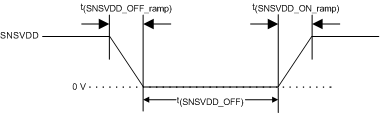 Figure 48. POR Sequence
Table 17. Requested POR Timings
| TEMPERATURE RANGE | MINIMAL t(SNSVDD_OFF_ramp) | MINIMAL t(SNSVDD_ON_ramp) | MINIMAL t(SNSVDD_OFF)(1) |
|---|---|---|---|
| –40°C to –21°C | 12 kV/s | 12 kV/s | 1.2 s |
| –20°C to 85°C | 2 kV/s | 12 kV/s | 200 ms |
8.2.2.1.2 Requesting a Minimal t(SNSVDD_OFF) Time
The POR circuit of the TSC2013-Q1 device contains a capacitor that is charged when the device powers up which generates an internal reset signal. This capacitor is discharged after the TSC2013-Q1 supply is switched off. The TSC2013-Q1 device is designed for low-power operation, therefore the POR requires time to charge and discharge the capacitor, especially under cold temperatures (less than –20°C). If the SNSVDD off time is not sufficient, the device can lock up. Only a power recycle can resolve this lockup condition.
8.2.2.1.3 Requesting a Minimal t(SNSVDD_OFF_ramp) and t(SNSVDD_ON_ramp) Ramp
To ensure proper initialization of the TSC2013-Q1 device, the device must reach a certain voltage before the internal POR signal is released. If the power supply on the ramp is too slow the device can power up in a random state which can cause a lock up.
The capacitor inside the POR circuit must be discharged through the SNSVDD pin. To support a proper discharge when the TSC2013-Q1 supply is switched off, TI recommends to provide a low resistance path on the SNSVDD pin.
8.2.2.1.4 Hardware Reset
The hardware reset pin, RESET, is available to perform a system reset which resets the device if the pulse width meets the timing requirement (at least 10-µs wide and the SNSVDD/VREF or I/OVDD pin is greater than or equal to 1.6 V). Any reset pulse less than 5 µs is rejected. To accommodate the timing drift between devices because of process variation, a reset pulse width between 5 µs and 10 µs is not recognized and the result is undetermined. This situation should be avoided. A good reset pulse must be low for at least 10 µs (SNSVDD/VREF or I/OVDD pin is greater than or equal to 1.6 V). An internal spike filter rejects spikes up to 20 ns wide. See Figure 37 for the hardware reset timing diagram.
8.2.2.1.5 Software Reset
During normal operation a software reset can be sent by the host processor to the device by setting the SWRST bit (D1) to 1 in the control byte 1 (see Table 6).
8.2.2.2 Power Up Considerations
8.2.2.2.1 Power-Off Cycles During Normal Operation
The TSC2013-Q1 device is a low-power device and therefore switching the TSC2013-Q1 device off during normal operation is not needed nor recommended.
Every power cycle (power on → power off → power on) must meet the requirements described in the Power-On Reset section. If requirements cannot be met, TI recommends to issue a hardware reset after every power cycle.
8.2.2.2.2 Supply Glitches During Normal Operation
A TSC2013-Q1 SNSVDD or IOVDD power glitch during normal operation can cause a lockup condition. Therefore ensure that the system is able to either recycle the power in the system following the requirements described in the Power-On Reset section or issue a hardware reset as described in the Hardware Reset section.
8.2.2.2.3 TSC2013-Q1 Digital Pins
In many applications, users use the same power supply for both the TSC2013-Q1 analog and digital supplies. The SNSVDD supply is connected with the I/OVDD supply. Under such cases, the logic high status on the TSC2013-Q1 digital pins before power-up become a concern when performing a proper POR.
Table 18 lists the digital I/O pins of the TSC2013-Q1 device.
Table 18. TSC2013-Q1 Digital Pin List
| TSC2013-Q1 PINS | DESCRIPTION |
|---|---|
| PINTDAV | Digital Output. Data available or the pen-detect interrupt (PENIRQ), depending on setting. Pin polarity is active-low. |
| RESET | Digital input. External hardware reset input (active-low). |
| SCL | Open drain and collector. Serial clock |
| SDA | Open drain and collector. Serial data I/O |
| A0 | Digital input. I2C bus TSC address input bit 0 |
| A1 | Digital input. I2C bus TSC address input bit 1 |
Every TSC2013-Q1 pin is well protected against ESD strikes. The TSC2013-Q1RESET, A0, and A1 pins have the same protection as the SDA and SCL pins. This protection allows the RESET, A0, and A1 pins to be pulled high before the device powers on without activating an internal ESD diode and without causing a power up of the TSC2013-Q1.
The output pin, PINTDAV, is a digital output pin. The host processor must define the PINTDAV pin as an input to the host processor without any pullup-pulldown feature. In some cases the default of the host processor is an output with an enabled pullup-pulldown feature but the host-processor firmware changes this definition at a later point to an input. If the TSC2013-Q1 device is not powered up, a power up can also occur through the ESD cells as shown in by the red line in Figure 49. This power up is considered a false power up. A false power up cannot ensure a proper power supply to the device or a proper POR.
In case the TSC2013-Q1 device is powered up, both the device and drive processor drive different levels on the same line resulting in high power consumption.
The TSC2013-Q1PINTDAV pin should be connected to the correct pin on the host processor to avoid bus conflicts and illegal powering up of the TSC2013-Q1 device.
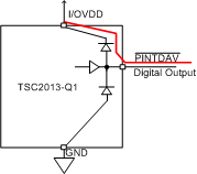 Figure 49. Internal ESD Protection Diodes at the TSC2013-Q1PINTDAV Pin
8.2.2.2.4 Suggested Hardware Reset During Power-On
The suggested sequence during power up is the following:
- Keep RESET pin low
- Wait for the supplies to settle
- Wait for at least 10µs before releasing the RESET pin
Figure 50 shows the suggested waveform.
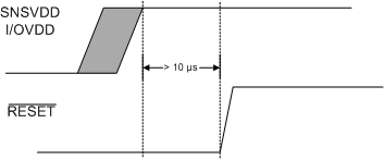 Figure 50. Suggested RESET Waveform During Power-On
8.2.2.3 Device Timing Setup and Use
The TSC2013-Q1 device is a register-based touch-screen controller (TSC). This section describes the setup and use of the programable timings available in the TSC2013-Q1 device.
Figure 52 through Figure 56 in the Application Curves were generated to show the principal. The TSC2013-Q1 X triplet contains X1, X2, and IX conversions. The TSC2013-Q1 Y triplet contains Y1, Y2, and IY conversions. The TSC2013-Q1 Z measurement contains Z1 and Z2 conversions.
8.2.2.3.1 Touch-Panel Driving Power
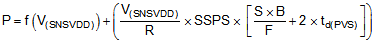
On a resistive touch-screen system, the driving current of the touch panel, provided by the TSC device through the analog interface, has the highest impact on the power consumption in the touch screen system. This touch-panel power consumption is decided by the resistance of the touch panel and the TSC power-supply (SNSVDD) voltage. Figure 51 shows this relationship. The touch screen is driven by the TSC from the SNSVDD supply and the resistance of the panel determines the peak drive current.
Figure 51 only shows the ideal TSC driving condition where the internal resistance of the TSC is ignored because the resistance is small (5 to 6 Ω) compared to the resistance of the touch panel (100s to 1000s Ω). Therefore the actual power consumption should be a little less than that shown in Figure 51.
A user can reduce power consumption in three ways:
- Using touch screens with higher resistance
- Using a low-power supply, SNSVDD, to the TSC
- Reducing the driver on-time or the on-off ratio of the driver
Touch panels with higher resistance are likely to cause more noise and longer settling time which limits the options for users.
The TSC20013-Q1 device is designed with a power supply, SNSVDD, range of 1.6 V to 3.6 V.
Reducing the driver on-time involves setting various touch-screen timings and delays. lists the relevant parameters concerning these timings and delays. The following sections describe the functions and effects of these timings and delays. See the Register Maps section for the timing settings of the configuration registers.
8.2.2.3.2 ADC Clock Effects
A TSC2013-Q1 device contains a nominal 4-MHz internal clock that is used to drive the state machines inside the device which performs the many functions. This clock is divided down to provide a clock to run the SAR ADC (analog-to-digital converter). If the 4-MHz clock is used directly (divided by 1), the ADC is limited to a 10-bit resolution, then using higher resolutions at this speed does not result in accurate conversions. The 12-bit resolution requires that the conversion clock run at either 2 MHz (divided by 2) or 1 MHz (divided by 4). The division ratio for the ADC clock is set in the configuration register 0 (CFR0), by setting the CL1 and CL0 bits (see Table 6).
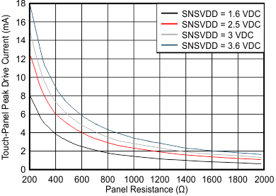
The ability to change the conversion clock rate allows the user to select the optimal value for the ADC resolution, speed, and power dissipation. Higher clock frequency results in faster touch-data converting speed and shorter touch-driver on-time which usually result in lower SNSVDD power consumption. Figure 52 and Figure 53 show examples of the ADC clock effect on the analog interface traffic (X+, X–, Y+, and Y– lines). In these figures, a TSC drives the touch panel to acquire the X, Y, Z1, and Z2 coordinates and three samples-per-coordinate. Figure 52 shows an analog interface with the clock frequency set to 2 MHz. Figure 53 shows an analog interface with the clock frequency set to 1-MHz. In Figure 52 and Figure 53, other than the ADC clock frequency difference, all other settings are completely identical with the following values: PVS equal to 0 µs, PR equal to 20 µs, and SN equal to 32 µs (see the Panel Voltage Stabilization Time section for more information on these timers).
The ADC clock frequency determines the length of the TSC acquisition time and TSC driver on-time. The faster the ADC clock, the shorter the driver on-time. For example, sampling 3 Y data with an ADC clock value of 2 MHz (see Figure 52) uses only about half of the time compared to sampling the data with an ADC clock value of 1 MHz (see Figure 53).
Use Equation 10 to calculate the analog power-supply current, I(SNSVDD).
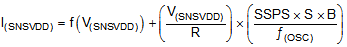
where
- f(V(SNSVDD)) is a function of V(SNSVDD)
- V(SNSVDD) is the SNSVDD voltage (in V)
- R is the average resistance of the touch panel (in Ω)
- SSPS is sample sets-per-second, which indicates how many sets of touch data is received by the host within a second
- S is the number of data in a set of samples
- B is the TSC resolution, either 10 bit or 12 bit
- ƒ(OSC) is ADC clock frequency, which can be 4, 2, or 1 MHz
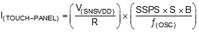
Equation 10 includes two parts: the internal circuitry power consumption or f(V(SNSVDD)) and the current to drive the external resistive-touch panel which is calculated using Equation 11.
A concern for using the faster ADC clock is because of the settling time or transients of the analog interface. The higher clock frequency can reduce the accuracy of the data in those cases where the TSC begins the data acquisitions before the analog interface lines reach the stable voltages. Therefore, adding some delays on the analog interface in order to wait for the interface to become stable before an ADC begins working might be necessary. These delays can include the panel voltage-stabilization time, the precharge time of the pins, the sense time (see the Panel Voltage Stabilization Time section), or a combination.
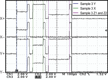
8.2.2.4 Panel Voltage Stabilization Time
The panel voltage-stabilization time, td(PVS), specifies a delay time from the moment the touch screen drivers are enabled to the time the voltage is sampled and a conversion is started. These bits allow the user to adjust the appropriate settling time for the touch panel based on the external capacitances at the analog interface lines.
Figure 54 shows examples where with td(PVS) is 0 µs (no PVS delay), 100 µs, and 500 µs. In the examples, the TSC uses the sets of 4 × 3 = 12 data which are 3 X, 3 Y, 3 Z1, and 3 Z2. The TSC2013-Q1 device always performs the Y coordinate first when it was set to X-Y or X-Y-Z scan mode. The sequence for receiving a set of samples in Figure 54 is as follows:
- The TSC adds driver power to Y+ (SNSVDD) and Y– (AGND), waits td(PVS) µs, and acquires 3 Y data
- The TSC adds driver power to X+ (SNSVDD) and X– (AGND), waits td(PVS) µs, and acquires 3 X data
- The TSC adds driver power to Y+ (SNSVDD) and X– (AGND), waits td(PVS) µs, and acquires 3 Z1 and 3 Z2 data
The PVS delay consumes power because a driver is on during the PVS delay. Use Equation 12 to calculate the power.
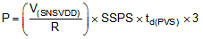
where
- 3 indicates that the X, Y, and Z drivers are on
Based on Equation 10, use Equation 13 to calculate a complete expression of the analog power consumption for X-Y-Z 3-dimension coordinates.

Use Equation 14 to calculate the power consumption for X-Y 2-dimension touch data.
where
- 2 indicates that the X and Y drivers are on
8.2.2.5 Precharge and Sense Time
Unlike the ADC clock frequency (bits CL1 to CL0) and panel voltage-stabilization time (bits PV2 to PV0), the other two TSC timings in the CFR0 register (see Table 6) affect the bus shape and traffic speed but do not effect power consumption of the analog interface.
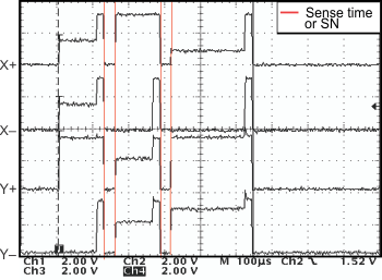
As shown in Figure 54, some added time or delays occur between samples of two coordinates such as after sampling Y and before the X driver turns on. This added time or delay is the precharge time (bits PR2 to PR0) and sense time (bits SN2 to SN0).
The precharge time sets the amount of time allowed for precharging any pin capacitance on the touch screen during TSC ADC conversions as shown in Figure 55.
The sense time sets the amount of delay for the TSC device to wait between two coordinates during TSC ADC conversions as shown in Figure 56.
If a pressure remains on the touch panel, the TSC devices can automatically and continuously acquire touch data. As many as several-thousand SSPS of touch data can be driven on, sampled, converted, and processed. For a typical application, however, users usually need only 100 to 500 SSPS of touch data because of the control and response limits of a human. To save power, users often do not want the system to acquire any unnecessary data.
The SSPS of a TSC can be reduced in several ways, including:
- Using the batch delay to add waiting time between the sets of touch data
- Inserting delays, such as PR and SN (but not PVS), to slow down the coordinate samples within a set because PR and SN do not consume power
See Table 6 for the bit locations and for the selectable time ranges.
8.2.2.6 Single-Touch Operation
The TSC2013-Q1 device can also be used only for single-touch operation. By measuring all 4-wire nodes (X+, X–, Y+, Y–) more-precise touch accuracy can be achieved compared to normal resistive TSCs.
TI advises to calculate the center point of the touch by using both node values. Equation 15 shows an example.
This same calculation method is used on dual-touch middle-point calculation.
8.2.3 Application Curves
ADC Clock = 1 MHz
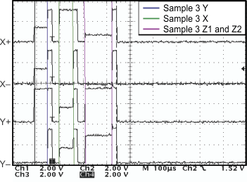
ADC Clock = 2 MHz
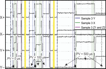
and 500 µs