ZHCSCV1A June 2014 – July 2014 TSC2013-Q1
PRODUCTION DATA.
- 1 特性
- 2 应用
- 3 说明
- 4 修订历史记录
- 5 Pin Configurations and Functions
-
6 Specifications
- 6.1 Absolute Maximum Ratings
- 6.2 Handling Ratings
- 6.3 Recommended Operating Conditions
- 6.4 Thermal Information
- 6.5 Electrical Characteristics
- 6.6 Timing Requirements — I2C Standard Mode (ƒ(SCL) = 100 kHz)
- 6.7 Timing Requirements — I2C Fast Mode (ƒ(SCL) = 400 kHz)
- 6.8 Timing Requirements — I2C High-Speed Mode (ƒ(SCL) = 1.7 MHz)
- 6.9 Timing Requirements — I2C High-Speed Mode (ƒ(SCL) = 3.4 MHz)
- 6.10 Typical Characteristics
-
7 Detailed Description
- 7.1 Overview
- 7.2 Functional Block Diagram
- 7.3 Feature Description
- 7.4 Device Functional Modes
- 7.5 Programming
- 7.6
Register Maps
- 7.6.1 Configuration and Status Registers
- 7.6.2 Data Registers
-
8 Application and Implementation
- 8.1 Application Information
- 8.2
Typical Application
- 8.2.1 Design Requirements
- 8.2.2 Detailed Design Procedure
- 8.2.3 Application Curves
- 9 Power Supply Recommendations
- 10Layout
- 11器件和文档支持
- 12机械封装和可订购信息
封装选项
机械数据 (封装 | 引脚)
散热焊盘机械数据 (封装 | 引脚)
- RSA|16
订购信息
6 Specifications
6.1 Absolute Maximum Ratings(1)
Over operating free-air temperature range (unless otherwise noted).| MIN | MAX | UNIT | |||
|---|---|---|---|---|---|
| Voltage | Analog input X+, Y+, AUX to SNSGND | –0.4 | SNSVDD + 0.1 | V | |
| Analog input X–, Y– to SNSGND | –0.4 | SNSVDD + 0.1 | V | ||
| SNSVDD to SNSGND | –0.3 | 5 | V | ||
| SNSVDD to AGND | –0.3 | 5 | V | ||
| I/OVDD to AGND | –0.3 | 5 | V | ||
| SNSVDD to I/OVDD | –2.4 | 0.3 | V | ||
| Digital input voltage to AGND | –0.3 | I/OVDD + 0.3 | V | ||
| Digital output voltage to AGND | –0.3 | I/OVDD + 0.3 | V | ||
| Power dissipation | (TJmax – TA) / RθJA | ||||
| Operating free-air temperature range, TA | –40 | 125 | °C | ||
| Junction temperature, TJmax | 150 | °C | |||
(1) Stresses beyond those listed under Absolute Maximum Ratings may cause permanent damage to the device. These are stress ratings only, and functional operation of the device at these or any other conditions beyond those indicated is not implied. Exposure to absolute-maximum rated conditions for extended periods may affect device reliability.
6.2 Handling Ratings
| MIN | MAX | UNIT | ||||
|---|---|---|---|---|---|---|
| Tstg | Storage temperature range | –65 | 150 | °C | ||
| V(ESD) | Electrostatic discharge | Human body model (HBM), per AEC Q100-002(1) | –2000 | 2000 | V | |
| Charged device model (CDM), per AEC Q100-011 | Corner pins (RSA: 1, 4, 5, 8, 9, 12, 13, and 16; PW: 1, 8, 9, and 16) |
–750 | 750 | |||
| Other pins | –500 | 500 | ||||
| IEC contact discharge(2) | X+, X–, Y+, Y– | –15 | 15 | kV | ||
| IEC air discharge(2) | X+, X–, Y+, Y– | –25 | 25 | kV | ||
(1) AEC Q100-002 indicates HBM stressing is done in accordance with the ANSI/ESDA/JEDEC JS-001 specification.
(2) Test method based on IEC standard 61000-4-2. Contact Texas Instruments for test details.
6.3 Recommended Operating Conditions
over operating free-air temperature range (unless otherwise noted)| MIN | NOM | MAX | UNIT | |
|---|---|---|---|---|
| Input voltage SNSVDD/VR | 1.6 | 3.3 | 3.6 | V |
| Input voltage I/OVDD | 1.2 | 3.3 | 3.6 | V |
6.4 Thermal Information
| THERMAL METRIC(1) | RSA | PW | UNIT | |
|---|---|---|---|---|
| 16 PINS | 16 PINS | |||
| RθJA | Junction-to-ambient thermal resistance | 33.7 | 100.9 | °C/W |
| RθJC(top) | Junction-to-case(top) thermal resistance | 36.7 | 36.1 | °C/W |
| RθJB | Junction-to-board thermal resistance | 10.5 | 45.7 | °C/W |
| ψJT | Junction-to-top characterization parameter | 0.6 | 2.6 | °C/W |
| ψJB | Junction-to-board characterization parameter | 10.5 | 45.1 | °C/W |
| RθJC(bot) | Junction-to-case(bottom) thermal resistance | 2.5 | — | °C/W |
(1) For more information about traditional and new thermal metrics, see the IC Package Thermal Metrics application report, SPRA953.
6.5 Electrical Characteristics
At TA = –40°C to 125°C, V(SNSVDD/VREF) = 1.6 V to 3.6 V, and V(I/OVDD)(2) = 1.2 V to V(SNSVDD/VREF), unless otherwise noted.| PARAMETER | TEST CONDITIONS | MIN | TYP | MAX | UNIT | |||
|---|---|---|---|---|---|---|---|---|
| AUXILIARY ANALOG INPUT | ||||||||
| Input voltage | 0 | Vref | V | |||||
| Input capacitance | 12 | pF | ||||||
| Input leakage current | No ADC conversion | –1 | 1 | μA | ||||
| Full-scale average input current | V(SNSVDD/VREF) = 1.6 V, continuous AUX, ƒ(ADC) = 2 MHz | 2 | μA | |||||
| ADC | ||||||||
| Resolution | Programmable: 10 or 12 bits | 12 | Bits | |||||
| No missing codes | 12-bit resolution | 11 | Bits | |||||
| Integral linearity | 12-bit resolution mode, ƒ(ADC) = 2 MHz | –3 | –0.5 to 0.5 | 3 | LSB(1) | |||
| Differential linearity | 12-bit resolution mode, fADC = 2MHz | –2 | –0.5 to 0.5 | 4 | LSB | |||
| Offset error | V(SNSVDD/VREF) = 1.6 V, 12-bit mode, ƒ(ADC) = 2 MHz, filter off | 0.2 | LSB | |||||
| Gain error | V(SNSVDD/VREF) = 1.6 V, 12-bit mode, ƒ(ADC) = 2 MHz, filter off | 2 | LSB | |||||
| Data format | Straight binary | |||||||
| REFERENCE INPUT | ||||||||
| Vref range | 1.6 | V(SNSVDD/VREF) | V | |||||
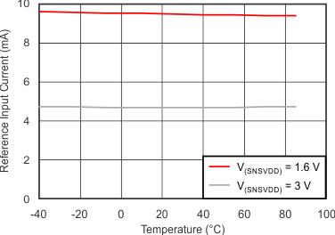
| SNSVDD/VREF input-current drain | Continuous AUX mode, V(SNSVDD/VREF) = 1.6 V, ƒ(ADC) = 2 MHz | 5 | μA | |||||
| Input impedance | No ADC conversion | > 100 | MΩ | |||||
| TOUCH SENSORS | ||||||||
| X+ 50-kΩ pullup resistor, R(IRQ) | 52 | kΩ | ||||||
| Switch on-resistance | Y+, X+ | TA = 25°C, V(SNSVDD/VREF) = 1.6 V | 7 | Ω | ||||
| Y–, X– | TA = 25°C, V(SNSVDD/VREF) = 1.6 V | 5 | Ω | |||||
| Switch drivers drive current | 100-ms duration | 50 | mA | |||||
| INTERNAL OSCILLATOR | ||||||||
| ƒ(OSC) | Clock frequency | V(SNSVDD/VREF) = 1.6 V, TA = 25°C | 3.3 | 3.7 | 4.3 | MHz | ||
| V(SNSVDD/VREF) = 3 V, TA = 25°C | 3.8 | MHz | ||||||
| Frequency drift | V(SNSVDD/VREF) = 1.6 V | –0.008 | %/°C | |||||
| V(SNSVDD/VREF) = 3 V | –0.021 | %/°C | ||||||
| DIGITAL INPUT/OUTPUT | ||||||||
| Logic family | CMOS | |||||||
| VIH | Input-voltage logic-level high | 1.2 V ≤ V(I/OVDD) < 3 V | 0.7 × V(I/OVDD) | 3.6 | V | |||
| VIL | Input-voltage logic-level low | 1.2 V ≤ V(I/OVDD) < 3 V | –0.3 | 0.2 × V(I/OVDD) | V | |||
| IIL, IIH | Input-current logic-level low and high | –1 | 1 | μA | ||||
| CI | Input-capacitance logic level | 10 | pF | |||||
| VOH | Output-voltage logic-level high | IOH = 100 μA | V(I/OVDD) – 0.2 | V(I/OVDD) | V | |||
| VOL | Output-voltage logic-level low | IOL = –3.2 mA | 0 | 0.2 | V | |||
| Ilkg | Leakage-current logic level | SDA | –1 | 1 | μA | |||
| CO | Output-capacitance logic level | SDA | 10 | pF | ||||
| POWER-SUPPLY REQUIREMENTS | ||||||||
| Power-supply voltage | ||||||||
| SNSVDD | 1.6 | 3 | V | |||||
| I/OVDD(2) | 1.2 | V(SNSVDD/VREF) | V | |||||
| Quiescent supply current(3)(4) |
TA = 25°C, filter off, M = W = 1, C[3:0] = (1, 0, 0, 0), RM = 1, CL[1:0] = (0, 1), cont AUX mode, ƒ(ADC) = 2 MHz, without reading data register | V(SNSVDD/VREF) = V(I/OVDD) = 1.6 V | 420 | 570 | μA | |||
| TA = 25°C, filter on, M = 15, W = 7, PSM = 1, C[3:0] = (0, 0, 0, 0), RM = 1, CL[1:0] = (0, 1), BTD[2:0] = (1, 0, 1), 50 SSPS, MAVEX = MAVEY = MAVEZ = 1, ƒ(ADC) = 2 MHz, sensor drivers supply included(5) | V(SNSVDD/VREF) = V(I/OVDD) = 1.6 V | 200 | μA | |||||
| V(SNSVDD/VREF) = V(I/OVDD) = 3 V | 400 | μA | ||||||
| TA = 25°C, filter off, M = W = 1, PSM = 1, C[3:0] = (0, 0, 0, 0), RM = 1, CL[1:0] = (0, 1), BTD[2:0] = (1, 0, 1), 50 SSPS, MAVEX = MAVEY = MAVEZ = 1, ƒ(ADC) = 2 MHz, sensor drivers supply included(5) | V(SNSVDD/VREF) = V(I/OVDD) = 1.6 V | 180 | μA | |||||
| V(SNSVDD/VREF) = V(I/OVDD) = 3 V | 370 | μA | ||||||
| TA = 25°C, filter off, M = W = 1, C[3:0] = (0, 1, 0, 1), RM = 1, CL[1:0] = (0, 1), non-cont AUX mode, ƒ(ADC) = 2 MHz, high-speed mode | V(SNSVDD/VREF) = V(I/OVDD) = 1.6 V, approximately 28 kSPS effective rate | 190 | μA | |||||
| V(SNSVDD/VREF) = V(I/OVDD) = 3 V, approximately 28.4 kSPS effective rate | 370 | μA | ||||||
| TA = 25°C, filter on, M = 7, W = 3, C[3:0] = (0, 1, 0, 1), RM = 1, CL[1:0] = (0, 1), MAVEAUX = 1, non-cont AUX mode, ƒ(ADC) = 2 MHz, high-speed mode, full speed | V(SNSVDD/VREF) = V(I/OVDD) = 1.6 V, approximately 10.5 kSPS effective rate | 355 | μA | |||||
| V(SNSVDD/VREF) = V(I/OVDD) = 3 V, approximately 10.9 kSPS effective rate | 655 | μA | ||||||
| TA = 25°C, filter on, M = 7, W = 3, C[3:0] = (0, 1, 0, 1), RM = 1, CL[1:0] = (0, 1), MAVEAUX = 1, non-cont AUX mode, ƒ(ADC) = 2 MHz, high-speed mode, reduced speed (8.2-kSPS equivalent rate) | V(SNSVDD/VREF) = V(I/OVDD) = 1.6 V, approximately 1.17 kSPS effective rate | 36.2 | μA | |||||
| V(SNSVDD/VREF) = V(I/OVDD) = 3 V, approximately 1.17 kSPS effective rate | 64.9 | μA | ||||||
| Power-down supply current | TA = 25°C, not addressed, SCL = SDA = 1, RESET = 1, PINTDAV = 1, V(SNSVDD/VREF) = I/OVDD = Vref = 1.6 V |
0.04 | 0.8 | μA | ||||
| Digital power-down supply current | TA = 25°C, not addressed, SCL = SDA = 1, RESET = 1, PINTDAV = 1, V(SNSVDD/VREF) = V(I/OVDD) = Vref = 1.6 V |
0.04 | 0.8 | μA | ||||
(1) LSB means least-significant bit. With SNSVDD/VREF= 2.5 V, one LSB is 610 μV.
(2) I/OVDD must be ≤ SNSVDD.
(3) Supply current from SNSVDD.
(4) For detailed information on test condition parameter and bit settings, see the section.
(5) Touch sensor modeled by 2 kΩ for X– plane and Y– plane, and 1 kΩ for Z-plane (touch resistance).
6.6 Timing Requirements — I2C Standard Mode (ƒ(SCL) = 100 kHz)
All specifications typical at –40°C to 125°C, V(SNSVDD/VREF) = V(I/OVDD) = 1.6 V to 3 V, unless otherwise noted.| MIN | MAX | UNIT | |||
|---|---|---|---|---|---|
| t(WL_RESET) | Reset low time(1) | See Figure 1 and Figure 37 | 10 | μs | |
| ƒ(SCL) | SCL clock frequency | 100 | kHz | ||
| t(BUF) | Bus free time between a STOP and START condition | See Figure 1 | 4.7 | μs | |
| th(STA) | Hold time for (repeated) START condition | 4 | μs | ||
| t(LOW) | Low period of SCL clock | 4.7 | μs | ||
| t(HIGH) | High period of the SCL clock | 4 | μs | ||
| tsu(STA) | Setup time for a repeated START condition | 4.7 | μs | ||
| th(DAT) | Data hold time | 0 | 3.45 | μs | |
| tsu(DAT) | Data setup time | 250 | ns | ||
| tr | Rise time of both SDA and SCL signals | C(b) = total bus capacitance See Figure 1 |
1000 | ns | |
| tf | Fall time of both SDA and SCL signals | 300 | ns | ||
| tsu(STO) | Setup time for STOP condition | See Figure 1 | 4 | μs | |
| C(b) | Capacitive load for each bus line | C(b) = total capacitance of one bus line in pF | 400 | pF | |
| td(SP) | Pulse duration of spikes that must be suppressed by the input filter | N/A | N/A | ns | |
(1) V(SNSVDD/VREF) ≥ 1.6 V
6.7 Timing Requirements — I2C Fast Mode (ƒ(SCL) = 400 kHz)
All specifications typical at –40°C to 125°C, V(SNSVDD/VREF) = V(I/OVDD) = 1.6 V to 3 V, unless otherwise noted.| MIN | MAX | UNIT | |||
|---|---|---|---|---|---|
| t(WL_RESET) | Reset low time(2) | See Figure 1 and Figure 37 | 10 | μs | |
| ƒ(SCL) | SCL clock frequency | 400 | kHz | ||
| t(BUF) | Bus free time between a STOP and START condition | See Figure 1 | 1.3 | μs | |
| th(STA) | Hold time for (repeated) START condition | 0.6 | μs | ||
| t(LOW) | Low period of SCL clock | 1.3 | μs | ||
| t(HIGH) | High period of the SCL clock | 0.6 | μs | ||
| tsu(STA) | Setup time for a repeated START condition | 0.6 | μs | ||
| th(DAT) | Data hold time | 0 | 0.9 | μs | |
| tsu(DAT) | Data setup time | 100 | ns | ||
| tr | Rise time of both SDA and SCL signals | C(b) = total bus capacitance See Figure 1 |
20 + 0.1 × C(b) | 300 | ns |
| tf | Fall time of both SDA and SCL signals(1) | 20 + 0.1 × C(b) | 300 | ns | |
| tsu(STO) | Setup time for STOP condition | See Figure 1 | 0.6 | μs | |
| C(b) | Capacitive load for each bus line | C(b) = total capacitance of one bus line in pF | 400 | pF | |
| td(SP) | Pulse duration of spikes that must be suppressed by the input filter | 0 | 50 | ns | |
(1) C(b) = the total capacitance of one bus line in pF. If using both fast-mode and Hs-mode devices, one may use faster fall times according to the Timing Requirements — I2C High-Speed Mode (ƒ(SCL) = 3.4 MHz) section. Note that the TSC2013-Q1 device is an Hs-mode device and follows the table requirements listed in the Timing Requirements — I2C High-Speed Mode (ƒ(SCL) = 3.4 MHz) section.
(2) V(SNSVDD/VREF) ≥ 1.6 V
6.8 Timing Requirements — I2C High-Speed Mode (ƒ(SCL) = 1.7 MHz)
All specifications typical at –40°C to 125°C, V(SNSVDD/VREF) = V(I/OVDD) = to 3 V, unless otherwise noted.| MIN | MAX | UNIT | |||
|---|---|---|---|---|---|
| t(WL_RESET) | Reset low time(2) | See Figure 2 and Figure 37 | 10 | μs | |
| ƒ(SCL) | SCL clock frequency | 1.7 | MHz | ||
| th(STA) | Hold time of (repeated) START condition | See Figure 2 | 160 | ns | |
| t(LOW) | Low period of SCL clock | 320 | ns | ||
| t(HIGH) | High period of the SCL clock | 120 | ns | ||
| tsu(STA) | Setup time for a repeated START condition | 160 | ns | ||
| th(DAT) | Data hold time | 0 | 150 | ns | |
| tsu(DAT) | Data setup time | 10 | ns | ||
| tr(CL) | Rise time of SCL signal | C(b) = total bus capacitance(1)
Figure 2 |
20 | 80 | ns |
| tr(DA) | Rise time of SDA signal | 20 | 160 | ns | |
| tf(CL) | Fall time of SCL signal | 20 | 80 | ns | |
| tf(DA) | Fall time of SDA signal | 1 | 160 | ns | |
| tr(CL1) | Rise time of SCL signal after a repeated START condition and after an acknowledge bit | 20 | 160 | ns | |
| tsu(STO) | Setup time for STOP condition | See Figure 2 | 160 | ns | |
| C(b) | Capacitive load for each bus line | C(b) = total capacitance of one bus line in pF | 400 | pF | |
| td(SP) | Pulse duration of spikes that must be suppressed by the input filter | 0 | 10 | ns | |
(1) For capacitive bus loads between 100 pF and 400 pF, interpolate the rise-time and fall-time values linearly.
(2) V(SNSVDD/VREF) ≥ 1.6 V
6.9 Timing Requirements — I2C High-Speed Mode (ƒ(SCL) = 3.4 MHz)
All specifications typical at –40°C to 125°C, V(SNSVDD/VREF) = V(I/OVDD) = 1.6 V(1) to 3 V, unless otherwise noted.| MIN | MAX | UNIT | |||
|---|---|---|---|---|---|
| t(WL_RESET) | Reset low time(3) | See Figure 2 and Figure 37 | 10 | μs | |
| ƒ(SCL) | SCL clock frequency | 3.4 | MHz | ||
| th(STA) | Hold time for (repeated) START condition | See Figure 2 | 160 | ns | |
| t(LOW) | Low period of SCL clock | 160 | ns | ||
| t(HIGH) | High period of the SCL clock | 60 | ns | ||
| tsu(STA) | Setup time for a repeated START condition | 160 | ns | ||
| th(DAT) | Data hold time | 0 | 70 | ns | |
| tsu(DAT) | Data setup time | 10 | ns | ||
| tr(CL) | Rise time of SCL signal | C(b) = total bus capacitance(2)
See Figure 2 |
10 | 40 | ns |
| tr(DA) | Rise time of SDA signal | 10 | 80 | ns | |
| tf(CL) | Fall time of SCL signal | 10 | 40 | ns | |
| tf(DA) | Fall time of SDA signal | 1 | 80 | ns | |
| tr(CL1) | Rise time of SCL signal after a repeated START condition and after an acknowledge bit | 10 | 80 | ns | |
| tsu(STO) | Setup time for STOP condition | See Figure 2 | 160 | ns | |
| C(b) | Capacitive load for each bus line | C(b) = total capacitance of one bus line in pF | 100 | pF | |
| td(SP) | Pulse duration of spikes that must be suppressed by the input filter | 0 | 10 | ns | |
(1) Because of the low supply voltage of 1.2 V and the wide temperature range of –40°C to 125°C, the I2C system devices may not reach the maximum specification of I2C high-speed mode, and ƒ(SCL) may not reach 3.4 MHz.
(2) Capacitive load from 10 pF to 100 pF.
(3) V(SNSVDD/VREF) ≥ 1.6 V
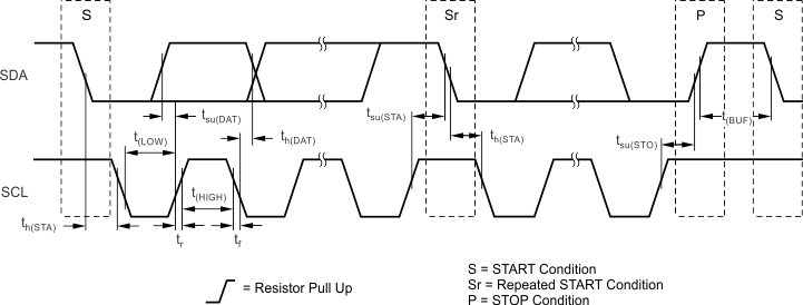 Figure 1. Detailed I/O Timing for Standard and Fast Modes
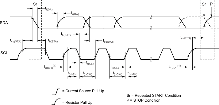
1. The First rising edge of the SCL signal after Sr and after each acknowledge bit.
Figure 2. Detailed I/O Timing for High-Speed Mode
6.10 Typical Characteristics
At TA = –40°C to 125°C, SNSVDD/VREF = 1.6 V to 3 V, I/OVDD = 1.2 V to SNSVDD/VREF, ƒ(ADC) = ƒ(OSC) / 2, high-speed mode (ƒ(SCL) = 3.4 MHz), 12-bit mode, and non-continuous AUX measurement, unless otherwise noted.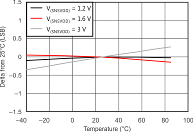 Figure 3. Change in Offset vs Temperature
| M = 1 | W = 1 (See Table 1) | ƒ(SAMPLE) = 28 kHz |
| AUX non-continuous mode | ||
| t(PVS), t(PRE), t(SNS) = default values | ||
| TSC-initiated mode scan X, Y, and Z at 50SSPS | ||
| Touch sensor modeled by: 2 kΩ for X-plane and Y-plane and 1 kΩ for Z (touch resistance, See Figure 14) |
| TA = 25°C | ||
| IOVDD = SNSVDD/VREF | ƒ(SAMPLE) = 28 kHz | |
| IOVDD = SNSVDD/VREF | AUX continuous mode | |||
| TA = 25°C | ||||
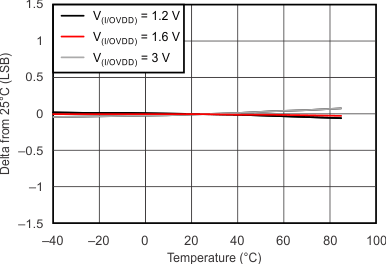 Figure 4. Change in Gain vs Temperature
| TA = 25° C | ||
| I/OVDD = SNSVDD/VREF | ||
| IOVDD = SNSVDD/VREF | AUX continuous mode | |