ZHCSCV1A June 2014 – July 2014 TSC2013-Q1
PRODUCTION DATA.
- 1 特性
- 2 应用
- 3 说明
- 4 修订历史记录
- 5 Pin Configurations and Functions
-
6 Specifications
- 6.1 Absolute Maximum Ratings
- 6.2 Handling Ratings
- 6.3 Recommended Operating Conditions
- 6.4 Thermal Information
- 6.5 Electrical Characteristics
- 6.6 Timing Requirements — I2C Standard Mode (ƒ(SCL) = 100 kHz)
- 6.7 Timing Requirements — I2C Fast Mode (ƒ(SCL) = 400 kHz)
- 6.8 Timing Requirements — I2C High-Speed Mode (ƒ(SCL) = 1.7 MHz)
- 6.9 Timing Requirements — I2C High-Speed Mode (ƒ(SCL) = 3.4 MHz)
- 6.10 Typical Characteristics
-
7 Detailed Description
- 7.1 Overview
- 7.2 Functional Block Diagram
- 7.3 Feature Description
- 7.4 Device Functional Modes
- 7.5 Programming
- 7.6
Register Maps
- 7.6.1 Configuration and Status Registers
- 7.6.2 Data Registers
-
8 Application and Implementation
- 8.1 Application Information
- 8.2
Typical Application
- 8.2.1 Design Requirements
- 8.2.2 Detailed Design Procedure
- 8.2.3 Application Curves
- 9 Power Supply Recommendations
- 10Layout
- 11器件和文档支持
- 12机械封装和可订购信息
封装选项
机械数据 (封装 | 引脚)
散热焊盘机械数据 (封装 | 引脚)
- RSA|16
订购信息
7 Detailed Description
7.1 Overview
The TSC2013-Q1 device is an analog interface circuit for a human-interface touch-screen device. A register-based architecture eases integration with microprocessor-based systems through a standard I2C bus. Registers and onboard state machines control all peripheral functions. The TSC2013-Q1 features include:
- Very low-power touch-screen controller
- Very small onboard footprint
- Flexible preprocessing which relieves the host from tedious routine tasks and saves resources for more critical tasks
- Ability to work on very low supply voltage
- Minimal connection interface allows easiest isolation and reduces the number of dedicated I/O pins required
- Enhanced ESD protection
- Panel-current sensing
- Miniature device, yet complete; requires no external supporting components
NOTE
Although the TSC2013-Q1 device can use an external reference, the SNSVDD/VREF pin can also be used as the reference.
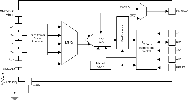
The TSC2013-Q1 device consists of the following blocks (see the Functional Block Diagram section):
- Touch-screen interface
- Auxiliary input (AUX)
- Acquisition-activity preprocessing
- Internal conversion clock
- I2C interface
Communication with the TSC2013-Q1 device is through an I2C serial interface. The TSC2013-Q1 device is an I2C slave device. Therefore, data shifts into or out of the TSC2013-Q1 device under the control of the host microprocessor, which also provides the serial data clock.
Writing to different registers in the TSC2013-Q1 device controls the TSC2013-Q1 device and device functions. The use of a simple command protocol (compatible with I2C) addresses these registers. This protocol can be an I2C write-address followed by multiple control bytes, or multiple combinations of control and data bytes for writing into different registers (two bytes each). To read from registers, write an I2C read-address to the TSC2013-Q1 device, followed by one or multiple sequential reads from the registers.
The host writes the address of the register to be read in control byte 0 with the register address and read-bit (as described in the previous paragraph). The register address serves as a pointer to the register map where the first read starts. This designated register address is static and a write to a register address does not need to occur again unless a new register address has overwritten it or after a TSC2013-Q1 reset (by a software reset or by the RESET pin).
The touch-measurement result goes into the TSC2013-Q1 registers, from which the host may read it at any time. This preprocessing frees up the host in order to allocate resources to more-critical tasks. Two optional signals are also available from the TSC2013-Q1 device to indicate that data are available for the host to read. The PINTDAV pin is a programmable interrupt or status output pin. With the PINTDAV pin programmed as a DAV output, the pin indicates that an ADC conversion has completed and that data are available. With the PINTDAV pin programmed as a PENIRQ output, the pin indicates the detection of a touch on the touch screen. The status register of the TSC2013-Q1 device provides an extended status reading, including the state of the DAV and PENIRQ outputs, without the cost of any dedicated pin. See Figure 14 for a typical application of the TSC2013-Q1 device.
To detect two touches, add an external R(SENSE) resistor as shown in Figure 14. The value of R(SENSE) depends on the touch-panel resistance. The ratio between the lowest touch-panel resistance and R(SENSE) should be approximately 4.5.
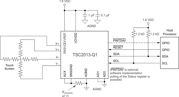 Figure 14. Typical Circuit Configuration
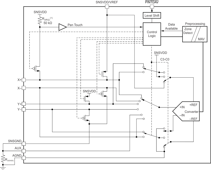
7.2 Functional Block Diagram
7.3 Feature Description
7.3.1 Touch-Screen Operation
A resistive touch screen operates by applying a voltage across a resistor network and measuring the change in resistance at a given point on the matrix where an input (stylus, pen, or finger) touches the screen. The change in the resistance ratio marks the location on the touch screen.
The TSC2013-Q1 device supports resistive 4-wire configurations as shown in Figure 15. The circuit determines location in two coordinate-pair dimensions, although addition of a third dimension for measuring pressure is possible.
7.3.2 4-Wire Touch Screen Measurements
Figure 15 shows construction of a typical four-wire touch screen. The screen consists of two transparent resistive layers separated by insulating spacers.
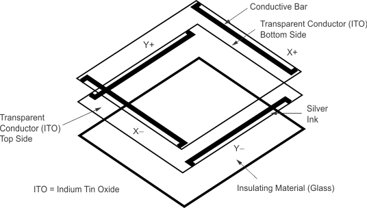 Figure 15. Four-Wire Touch Screen Construction
The four-wire touch-screen panel works by applying a voltage across the vertical or horizontal resistive network.
To determine a touch location, the TSC2013-Q1 device provides a set of eight data measurements (X1, X2, IX, Y1, Y2, IY, Z1, and Z2). Figure 17 through Figure 19 show the internal ADC configurations. Taking an X1 measurement involves activating the X+ and X– drivers and digitizing the voltage at Y+. The R(SENSE) resistor must be connected as shown in Figure 14. The SNSGND and AUX pins connect to one end of R(SENSE), and the other end connects to the AGND pin.
The TSC2013-Q1 device can also measure touch pressure (Z). To determine a pen or finger touch, determination of the pressure of the touch is required. Generally, having very high performance for this test is not necessary. Therefore, TI recommends 10-bit resolution mode. Several different ways of performing this measurement are available. The TSC2013-Q1 device supports two methods. The first method requires knowing the X-plate resistance, the measurement of X1, and two additional cross-panel measurements (Z2 and Z1) of the touch screen (see Figure 16). Equation 1 calculates the touch resistance (R(TOUCH)).
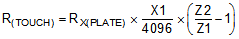
The second method requires knowing both the X-plate and Y-plate resistance, and the measurement of X1, Y1, and Z1. Equation 2 also calculates the touch resistance.
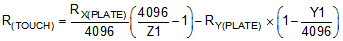
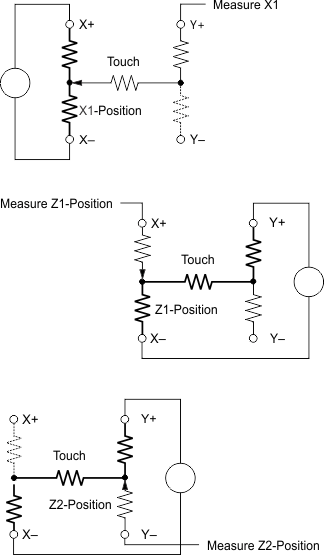 Figure 16. Pressure Measurement
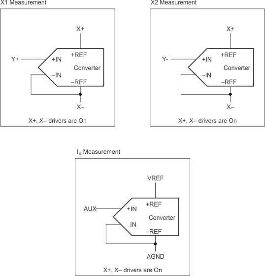 Figure 17. X-Coordinate Differential-Triplet Measurement (X1, X2, IX)
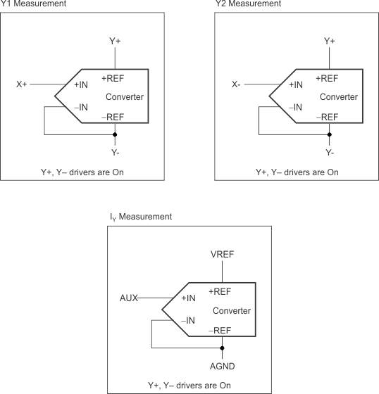 Figure 18. Y-Coordinate-Differential-Triplet Measurement (Y1, Y2, IY)
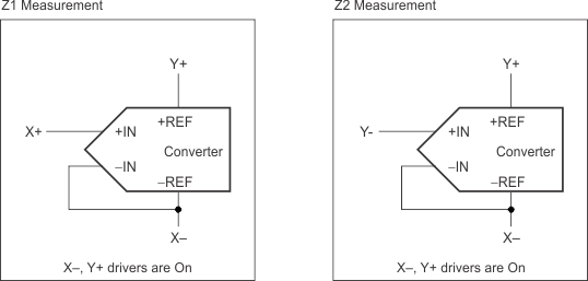 Figure 19. Z-Measurement (Z1, Z2)
When touching or pressing the touch panel with the drivers to the panel turned on, the voltage across the touch panel often overshoots and then slowly settles down (decays) to a stable DC value. This effect is a result of mechanical bouncing caused by vibration of the top-layer sheet of the touch panel when pressing the panel. Without accounting for this settling time, the converted value is in error. Therefore, introducing a delay between the time the driver for a particular measurement is turned on and the time a measurement is made is necessary.
In some applications, external capacitors may be required across the touch screen for filtering noise picked up by the touch screen (such as noise generated by the LCD panel or back-light circuitry). The value of these capacitors provides a low-pass filter to reduce noise, but causes an additional settling-time requirement when the panel is touched.
The TSC2013-Q1 device offers several solutions to this problem. A programmable delay time is available that sets the delay between turning the drivers on and making a conversion. The TSC2013-Q1 device uses this delay, referred to as the panel voltage-stabilization time, in some of the device modes. In other modes, commands can cause the TSC2013-Q1 device to turn on the drivers only without performing a conversion. Issuing the command to perform a conversion occurs after allowing sufficient stabilization time.
The TSC2013-Q1 touch-screen interface can measure different data sets. Determination of these measurements is possible under three different modes of the ADC:
- TSMode1: conversion controlled by the TSC2013-Q1 device and initiated by the touchscreen controller (TSC)
- TSMode2: conversion controlled by the TSC2013-Q1 device and initiated by the host responding to the PENIRQ signal
- TSMode3: conversion completely controlled by the host processor
7.3.3 Analog-to-Digital Converter
Figure 20 shows the analog inputs of the TSC2013-Q1 device. A multipexer provides the analog inputs (X, Y, and Z touch panel coordinates and auxiliary inputs) to the successive-approximation register (SAR) analog-to-digital converter (ADC). The basis of ADC architecture is capacitive redistribution architecture, which inherently includes a sample-and-hold function.
A unique configuration of low on-resistance switches allows an unselected ADC input channel to provide power and an accompanying pin to provide ground for driving the touch panel. By maintaining a differential input to the converter and a differential reference input architecture, negating errors caused by the on-resistance of the driver switches is possible.
Two ADC-control registers control the ADC. Several modes of operation are possible, depending on the bits set in the control registers. Programming of channel selection, scan operation, preprocessing, resolution, and conversion rate is through these registers. The following sections outline these modes for each type of analog input. The appropriate result register stores the conversion results.
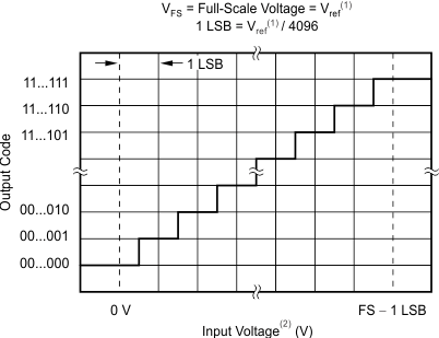
7.3.3.1 Data Format
The TSC2013-Q1 output data are in straight binary format as shown in Figure 21. Figure 21 shows the ideal output code for the given input voltage and does not include the effects of offset, gain, or noise.
7.3.3.2 Reference
The TSC2013-Q1 device uses an external voltage reference applied to the SNSVDD/VREF pin. Using the SNSVDD/VREF pin as the reference voltage is possible because the upper reference voltage range is the same as the supply-voltage range.
7.3.3.3 Variable Resolution
The TSC2013-Q1 device provides either 10-bit or 12-bit resolution for the ADC. Lower resolution is often practical for measuring slow-changing signals such as touch pressure. Performing the conversions at lower resolution reduces the amount of time required for the ADC to complete the conversion process which also lowers power consumption.
7.3.3.4 Conversion Clock and Conversion Time
The TSC2013-Q1 device contains an internal clock (oscillator) that drives the internal state machines that perform the many functions of the part. This clock is divided down to provide a conversion clock for the ADC. The setting for the division ratio of this clock is in the ADC control register (see Configuration Register 0 (address = 0) [reset = 4000h for read; 0000h for write]). The ability to change the conversion clock rate allows the user to select the optimal values for resolution, speed, and power dissipation. Using the 4-MHz (oscillator) clock directly as the ADC clock (when the CL[1:0] bit is set to 0) limits the ADC resolution to 10 bits. Using higher resolutions at this speed does not result in more accurate conversions. Twelve-bit resolution requires that the CL bits 1 and 0 are set to 0 and 1, or 1 and 0 (respectively).
Regardless of the conversion clock speed, the internal clock runs nominally at 3.8 MHz at a 3-V supply (SNSVDD) and slows down to 3.6 MHz at a 1.6-V supply. The conversion time of the TSC2013-Q1 device depends on several functions. The conversion clock speed plays an important role in the time required for a conversion to complete. However, proper sampling of the signal requires a certain number of internal clock cycles. Moreover, additional times (such as the panel voltage-stabilization time), can add significantly to the time it takes to perform a conversion. Conversion time can vary depending on the mode of use of TSC2013-Q1 device. This data sheet makes use of internal and conversion clock cycles throughout as the units used to describe the amount of time that many functions take. Take these times into account when considering the total system design.
7.3.3.5 Touch Detect
The PINTDAV pin can be programmed to generate an interrupt to the host. Figure 22 shows an example for a typical screen-touch situation. While in the power-down mode, the Y– driver is on and connects to GND. The internal pen-touch signal depends on whether or not the X+ input is low. A touch on the panel pulls the X+ input to ground through the touch screen and sets the internal pen-touch output to low because of the detection on the current path through the panel to ground, which initiates an interrupt to the processor. During the measurement cycles for X and Y-position, the device disconnects the X+ input, which eliminates any leakage current from the pullup resistor flowing through the touch screen, thus causing no errors.
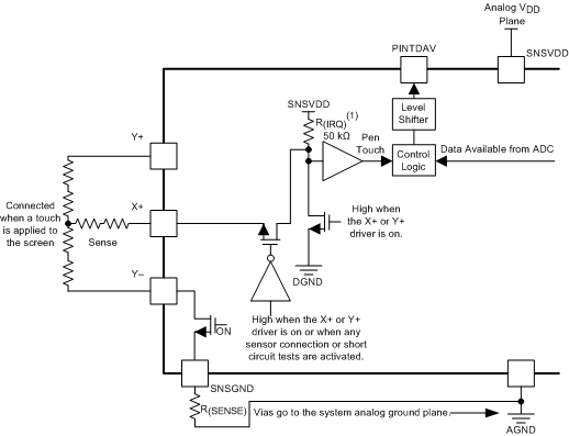
In modes where the TSC2013-Q1 device must detect whether or not a touch remains on the screen (for example, when doing a pen-touch-initiated X, Y, and Z conversion), the TSC2013-Q1 device must reset the drivers to connect the R(IRQ) resistor again. Because of the high value of this pullup resistor, any capacitance on the touch screen inputs causes a long delay time, and may prevent the detection from occurring correctly. To prevent this possible delay, the TSC2013-Q1 device has a circuit that allows prechargingd any screen capacitance, so that the pullup resistor must not be the only source for the charging current. The setting for the time allowed for this precharge, as well as the time needed to sense if the screen touch remains, is in the configuration register.
This configuration underscores the need to use the minimum possible capacitor values on the touch-screen inputs. Capacitors can be used to reduce noise, but capacitors with too large a value increase the required precharge and sense times, as well as the panel voltage-stabilization time.
7.3.3.6 Preprocessing
The TSC2013-Q1 device offers an array of powerful preprocessing operations that reduce unnecessary traffic on the bus and reduce the host processor loading. This reduction is especially critical for the serial interface because of the slow bus speed and the high CPU bandwidth required for I2C communication.
All data-acquisition tasks are looking for specific data that meet certain criteria. Many of these tasks fall into a predefined range, while other tasks may be looking for a value in a noisy environment. If the host processor is to retrieve all these data for processing, the limited bus bandwidth quickly saturates, along with the host processor processing capability. In any case, reserving the host processor for more critical tasks rather than routine work is always necessary.
The preprocessing unit consists of two main functions which result in the combined MAV (median and averaging-value) filter: the median value filter (MVF) and the averaging-value filter (AVF).
7.3.3.6.1 Preprocessing—Median Value Filter and Averaging Value Filter
The first preprocessing function, a combined MAV filter, can operate independently as a median value filter (MVF), an averaging value filter (AVF), and a combined filter (MAV filter).
If the acquired signal source is noisy because of the digital switching circuit, evaluating the data without noise may be necessary. In this case, the median value filter (MVF) operation helps to discard noise. The first action is sorting the array of N converted results. The return value is either the middle (median value) of an array of M converted results, or the average value of a window size of W of converted results:
-
N= the total number of converted results used by the MAV filter
-
M= the median value filter size programmed
-
W= the averaging window size programmed
If M is equal to 1, then N is equal to W. A special case is W equal to 1, which indicates a bypassed MAV filter. Otherwise, if W is greater than 1, averaging is the only function performed on these converted results. In either case, the return value is the averaged value of window size W of converted results.
If M is greater than 1 and W is equal to 1, then N is equal to M, meaning the only operating filter is the median value filter. The return value is the middle position converted result from the array of M converted results.
If M is greater than 1 and W is greater than 1, then N is equal to M. In this case, W is less than M. The return value is the averaged value of middle portion W of converted results out of the array of M converted results. Because the value of W is an odd number in this case, the calculation of the averaging value counts the middle-position converted result twice (averaging a total of W + 1 converted results).
Table 1. Median Value Filter-Size Selection
| M1 | M0 | MEDIAN VALUE FILTER M = |
POSSIBLE AVERAGING WINDOW SIZE W = |
|---|---|---|---|
| 0 | 0 | 1 | 1, 4, 8, 16 |
| 0 | 1 | 3 | 1 |
| 1 | 0 | 7 | 1, 3 |
| 1 | 1 | 15 | 1, 3, 7 |
Table 2. Averaging Value Filter-Size Selection
| AVERAGING VALUE FILTER SIZE SELECTION W = |
|||
|---|---|---|---|
| W1 | W0 | M = 1 (Averaging Only) | M > 1 |
| 0 | 0 | 1 | 1 |
| 0 | 1 | 4 | 3 |
| 1 | 0 | 8 | 7 |
| 1 | 1 | 16 | Reserved |
The device uses the default MVF setting (median value filter with averaging bypassed) for any invalid MAV filter configuration. For example, if M1, M0, W1, and W0 equals 1, 0, 1, and 0 (respectively), the MAV filter will perform as if it were configured for 1, 0, 0, 0, median filter only with filter size of 7, and no averaging. The only exception is when M is greater than 1 and when W1 and W0 equal 1. Avoid using this reserved setting.
Table 3. Combined MAV Filter Setting
| M | W | INTERPRETATION | N = | OUTPUT |
|---|---|---|---|---|
| = 1 | = 1 | Bypass both MAF and AVF | W | The converted result |
| = 1 | > 1 | Bypass MVF only | W | Average of W converted results |
| > 1 | = 1 | Bypass AVF only | M | Median of M converted results |
| > 1 | > 1 | M > W | M | Average of middle W of M converted results with the median counted twice |
The MAV filter is available for all analog inputs including the touch-screen inputs and the AUX measurement.
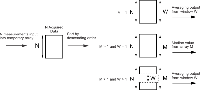 Figure 23. MAV Filter Operation
7.4 Device Functional Modes
7.4.1 Conversion Controlled by TSC2013-Q1 and Initiated by TSC2013-Q1 (TSMode 1)
In TSMode 1, before a pen-touch detection is possible, the TSC2013-Q1 device must be programmed with the PSM bit set to 1 and one of two scan modes:
- X-triplet, Y-triplet, Z-scan (converter function select bits C[3:0] = control byte 1 D[6:3] = 0000)
- IX-IY scan (converter function select bits C[3:0] = control byte 1 D[6:3] = 0001).
See Table 7 for more information on the converter function-select bits.
On touching the touch panel, the internal pen-touch signal activates, lowering the PINTDAV output if programmed as PENIRQ. The TSC2013-Q1 device then executes the preprogrammed scan function without a host intervention.
7.4.1.1 IX-IY Scan
The TSC2013-Q1 device starts up the internal clock. The device then turns on the Y-drivers, and after a programmed panel voltage-stabilization time, the device powers up the ADC and converts the IY coordinate. With preprocessing selected, several conversions can occur. When data preprocessing is complete, a temporary register stores the IY coordinate result.
If the screen touch remains at this time, the device enables the X-drivers and the process repeats but measures the IX coordinate instead, storing the result in a temporary register.
Figure 24 shows a flowchart for this process. The time required to go through this process depends on the selected resolution, internal conversion clock rate, panel voltage-stabilization time, precharge and sense times, and the selection status of preprocessing. Use Equation 3 to calculate the time required to achieve a complete X and Y coordinate (sample set) reading.

where
- t(COORDINATE) = time to complete IX and IY coordinate reading
- N = number of measurements for MAV filter input, as given in Table 3 as N
(For no MAV: M1 = M0 = W1 = W0 = 0) - t(PVS) = panel voltage stabilization time, as listed in Table 11
- t(PRE) = precharge time, as listed in Table 11
- t(SNS) = sense time, as listed in Table 11
- B = number of bits of resolution
- ƒ(OSC) = TSC onboard OSC clock frequency. See the Electrical Characteristics section for supply frequency (SNSVDD)
- ƒ(ADC) = ADC clock frequency, as listed in Table 11
- t(OH1) = overhead time number 1 = 2.5 internal clock cycles
- td(OH1) = total overhead time for t(PVS), t(PRE), and t(SNS) = 10 internal clock cycles
- tc(OH) = total overhead time for A-to-D conversion = 3 internal clock cycles
- t(PPRO) = preprocessor preprocessing time as listed in Table 4
Table 4. Preprocessing Delay
| t(PPRO) = | |||
|---|---|---|---|
| M = | W = | FOR B = 12 BIT | FOR B = 10 BIT |
| 1 | 1, 4, 8, 16 | 2 | 2 |
| 3, 7 | 1 | 28 | 24 |
| 7 | 3 | 31 | 27 |
| 15 | 1 | 31 | 29 |
| 15 | 3 | 34 | 32 |
| 15 | 7 | 38 | 36 |
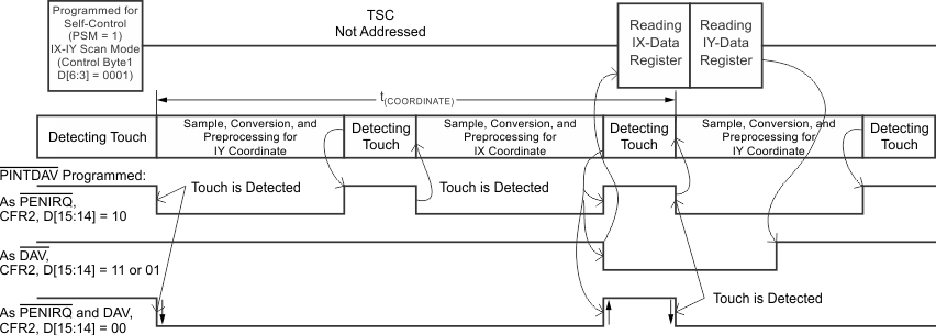 Figure 24. Example of an IX and IY Touch-Screen Scan Using TSMode 1
7.4.1.2 X-Triplet, Y-Triplet, Z-Scan
The TSC2013-Q1 device starts up the internal clock. The device then turns on the Y-drivers, and after a programmed panel voltage-stabilization time, powers up the ADC and converts the Y-triplet. With preprocessing selected, several conversions can occur. When data preprocessing is complete, temporary registers store the Y-triplet results.
If the screen touch remains at this time, the device enables the X-drivers and the process repeats but measures the X-triplet instead, storing the result in temporary registers.
The process continues in the same way, but measures the Z1 and Z2 values instead, storing the results in temporary registers. When the complete sample set of data (X1, X2, IX, Y1, Y2, IY, Z1, and Z2) are available, the device loads the data in the X1, X2, IX, Y1, Y2, IY, Z1, and Z2 registers. Figure 25 shows this process. This process time depends on the previously described settings. Use Equation 4 to calculate the time for a complete X1, X2, IX, Y1, Y2, IY, Z1, and Z2 coordinate reading.

where
- t(OH2) = overhead time number 2 = 3.5 internal clock cycles
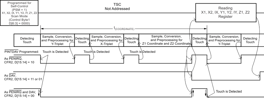 Figure 25. Example of an X-Triplet and Y-Triplet Coordinate Touch-Screen Scan Using TSMode 1
7.4.2 Conversion Controlled by TSC2013-Q1 and Initiated by Host (TSMode 2)
In TSMode 2, the TSC2013-Q1 device detects when a touch of the touch panel occurs and causes the internal pen-touch signal to activate, which lowers the PINTDAV output if programmed as PENIRQ. The host recognizes the interrupt request and then writes to the ADC control register to select one of the following two Touch-Screen Scan functions:
- X-triplet, Y-triplet, Z-scan (converter function select bits C[3:0] = control byte 1 D[6:3] = 0000); or
- IX-IY scan (converter function select bits C[3:0] = control byte 1 D[6:3] = 0001).
See Table 7 for more information on the converter function-select bits.
The conversion process then proceeds as shown in Figure 26. See the IX-IY Scan and X-Triplet, Y-Triplet, Z-Scan sections for additional details.
The main difference between this mode and the previous mode is that the host, not the TSC2013-Q1 device, decides when the touch-screen scan begins.
Use Equation 3 to calculate the time required to convert both IX and IY under host control (not including the time required to send the command over the I2C bus):
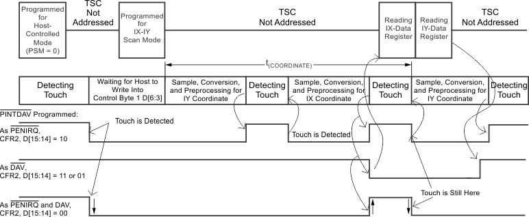 Figure 26. Example of an IX and IY Touch-Screen Scan Using TSMode 2
7.4.3 Conversion Controlled by Host (TSMode 3)
In TSMode 3, the TSC2013-Q1 device detects a touch of the touch panel and causes the internal pen-touch signal to be active, which lowers the PINTDAV output if programmed as PENIRQ. The host recognizes the interrupt request. Instead of starting a sequence in the TSC2013-Q1 device, which then reads each coordinate in turn, the host must now control all aspects of the conversion. Generally, on receiving the interrupt request, the host turns on the X drivers.
NOTE
With the drivers turned off, the device detects this condition and turns the driver on before the scan starts. This situation is why the event of turn on drivers is shown as optional in Figure 27 and Figure 29.
After waiting for the settling time, the host then addresses the TSC2013-Q1 device again, this time requesting an X-coordinate conversion.
The process then repeats for the Y and Z coordinates. Figure 27 and Figure 29 show this process. Figure 27 shows two consecutive scans on IX and IY. Figure 29 shows a single Z scan.
Use Equation 5 to calculate the time required to convert any single X-triplet or Y-triplet under host control (not including the time required to send the command over the I2C bus):

where
- td(OH2) = total overhead time for t(PRE) and t(SNS) = 6 internal clock cycles
(Without Panel Stabilization Time) Using TSMode 3
Use Equation 6 to calculate the time required to convert any single X-triplet or Y-triplet under host control (not including the time required to send the command over the I2C bus):

 Figure 28. Example of a Single X-Triplet Touch-Screen Scan
(With Panel Stabilization Time) Using TSMode 3
Use Equation 7 to calculate the time required to convert any Z1 and Z2 coordinate under host control (not including the time required to send the command over the I2C bus):

(Without Panel Stabilization Time) Using TSMode 3
If the drivers do not turn on prior to programming the touch-screen scan mode, include the panel stabilization time. In this case, use Equation 8 to calculate the time required to convert any single X or Y under host control (not including the time required to send the command over the I2C bus):

 Figure 30. Example of a Z1 and Z2 Coordinate Touch-Screen Scan
(With Panel Stabilization Time) Using TSMode 3
7.5 Programming
7.5.1 I2C Interface
The TSC2013-Q1 device supports the I2C serial bus and data transmission protocol in all three defined modes: standard, fast, and high-speed. A device that sends data onto the bus has the definition of a transmitter, and a device receiving data that of a receiver. The device that controls the message is a master. Devices controlled by the master are slaves. A master device that generates the serial clock (SCL), controls bus access, and generates the START and STOP conditions must control the bus The TSC2013-Q1 device operates as a slave on the I2C bus. Connections to the bus are through the open-drain I/O lines, SDA and SCL.
The following bus protocol has been defined (see Figure 31):
- A device can initiate data transfer only when the bus is not busy.
- During data transfer, the data line must remain stable whenever the clock line is high. Changes in the data line while the clock line is high are interpreted as control signals.
Accordingly, definitions for the following bus conditions follow:
-
Bus Not Busy Both data and clock lines remain high.
-
Start Data Transfer A change in the state of the data line, from high to low, while the clock is high, defines a start condition.
-
Stop Data Transfer A change in the state of the data line, from low to high, while the clock line is high, defines the stop condition.
-
Data ValidThe state of the data line represents valid data, when, after a start condition, the data line is stable for the duration of the high period of the clock signal. One clock pulse occurs per bit of data.
Each data transfer begins with a start condition and terminates with a stop condition. The number of data bytes transferred between start and stop conditions, which the master device determines, is not limited. The information transfers byte-wise, and the receiver acknowledges each byte with a ninth bit.
The I2C bus specifications define a standard mode (100-kHz clock rate), a fast mode (400-kHz clock rate), and a high-speed mode (3.4-MHz clock rate). The TSC2013-Q1 device works in all three modes.
-
AcknowledgeEach receiving device, when addressed, must generate an acknowledge after the reception of each byte. The master device must generate an extra clock pulse for association with this acknowledge bit.
A device that acknowledges must pull down the SDA line during the acknowledge clock pulse in such a way that the SDA line is stable low during the high period of the acknowledge clock pulse. Of course, the timing must take into account setup and hold times. A master must signal an end-of-data to the slave by not generating an acknowledge bit on the last byte that clocks out of the slave. In this case, the slave must leave the data line high to enable the master to generate the stop condition.
Figure 31 shows the data-transfer process on the I2C bus. Depending on the state of the R/W bit, two types of data transfer are possible:
- Data transfer from a master transmitter to a slave receiver.
- Data transfer from a slave transmitter to a master receiver.
The first byte transmitted by the master is the slave address. A number of data bytes occurs next. The slave returns an acknowledge bit after the slave address and each received byte.
The master transmits the first byte, the slave address. The slave then returns an acknowledge bit. Next, the slave transmits a number of data bytes to the master. The master returns an acknowledge bit after all received bytes other than the last byte. At the end of the last received byte, the master returns a not-acknowledge.
The master device generates all of the serial clock pulses and the start and stop conditions. A transfer ends with a stop condition or a repeated start condition. Because a repeated start condition is also the beginning of the next serial transfer, the bus is not released.
The TSC2013-Q1 device can operate in the following two modes:
- Slave receiver mode
- Slave transmitter mode
Reception of serial data and clock is through SDA and SCL. After the reception of each byte, the receiver transmits an acknowledge bit. Start and stop conditions designate the beginning and end of a serial transfer. Hardware performs address recognition after reception of the slave address and direction bit.
Reception and handling of the first byte (the slave address) is the same as in the slave receiver mode. However, in this mode the direction bit indicates a reversal of the transfer direction. Serial data transmission on SDA by the TSC2013-Q1 device occurs during input of the serial clock on SCL. Start and stop conditions designate the beginning and end of a serial transfer.
7.5.1.1 I2C Fast or Standard Mode (F-S Mode)
In I2C fast or standard (F-S) mode, serial data transfer must meet the timing shown in the timing requirement tables in the Specifications section.
In the serial transfer format of F-S mode, the master signals the beginning of a transmission to a slave with a start condition (S), which is a high-to-low transition on the SDA input while SCL is high. When the master has finished communicating with the slave, the master issues a stop condition (P), which is a low-to-high transition on SDA while SCL is high, as shown in Figure 31. The bus is free for another transmission after the occurrence of a stop. Figure 31 shows the complete F-S mode transfer on the I2C, two-wire serial interface. Transmission of the address byte, control byte, and data byte is between the start and stop conditions. The SDA state can only change while SCL is low, except for the start and stop conditions. Data transmission is in 8-bit words. Nine clock cycles are necessary to transfer the data into or out of the device (8-bit word plus acknowledge bit).
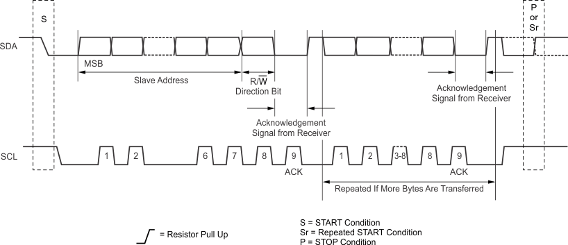 Figure 31. Complete Fast or Standard-Mode Transfer
7.5.1.2 I2C High-Speed Mode (Hs Mode)
Serial data transfer format in high-speed (Hs) mode meets the fast or standard (F-S) mode I2C bus specification. Hs mode can only commence after the following conditions (all of which are in F-S mode) exist:
- Start condition (S)
- 8-bit master code (0000 1xxx)
- Not-acknowledge bit (N)
Figure 32 shows this sequence in more detail. Hs-mode master codes are reserved 8-bit codes used only for triggering Hs mode. Do not use these codes for slave addressing or any other purpose. The master code indicates to other devices that an Hs-mode transfer is about to begin and the connected devices must meet the Hs mode specification. Because no device can acknowledge the master code, a not-acknowledge bit (N) follows the master code.
After the not-acknowledge bit (N) and SCL achieve a high level, the master switches to Hs-mode and enables (at time t(H); shown in Figure 32) the current-source pullup circuit for SCL. Because other devices can delay the serial transfer before t(H) by stretching the LOW period of SCL, the master enables the current-source pullup circuit when all devices have released SCL and SCL has reached a high level, thus speeding up the last part of the rise time of the SCL.
The master then sends a repeated start condition (Sr) followed by a 7-bit slave address with an R/W bit address, and receives an acknowledge bit (A) from the selected slave. After a repeated start (Sr) condition and after each acknowledge bit (A) or not-acknowledge bit (N), the master disables the current-source pullup circuit. This disabling enables other devices to delay the serial transfer by stretching the low period of SCL. The master re-enables the current-source pullup circuit again when all devices have released, and SCL reaches a high level, which speeds up the last part of the SCL signal rise time.
Data transfer continues in Hs mode after the next repeated start (Sr), and only switches back to F-S mode after a stop condition (P). To reduce the overhead of the master code, the master can link to a number of Hs mode transfers, separated by repeated start conditions (Sr).
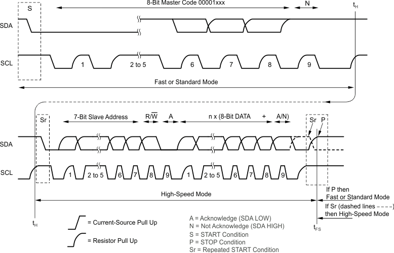 Figure 32. Complete High-Speed Mode Transfer
7.5.2 Digital Interface
7.5.2.1 Address Byte
The TSC2013-Q1 device has a 7-bit slave address word. The factory presets the first five bits (MSBs) of the slave address to comply with the I2C standard for ADCs; the setting is always 1 0010. The logic state of the address input pins (AD1 through AD0) determines the two LSBs of the device address to activate communication. Therefore, one bus can accommodate a maximum of four devices with the same preset code at one time.
The device only reads the AD1 through AD0 address inputs during a power-up of the device, and the pin connections should be to a digital supply (I/OVDD) or digital ground (DGND). The TSC2013-Q1 latches the slave address on the falling edge of SCL after reception of the R/W bit by the slave.
The last bit of the address byte (R/W) defines the operation to be performed. Setting the bit to 1 selects a read operation. Setting the bit to 0 selects a write operation. Following the start condition, the TSC2013-Q1 device monitors the SDA bus, checking the transmitted device-type identifier. On receiving the 1 0010 code, the appropriate device select bits, and the R/W bit, the slave device outputs an acknowledge signal on the SDA line.
Table 5. I2C Slave Address Byte
| MSB D7 |
D6 | D5 | D4 | D3 | D2 | D1 | LSB D0 |
|---|---|---|---|---|---|---|---|
| 1 | 0 | 0 | 1 | 0 | AD1 | AD0 | R/W |
| R/W (D0) |
1: I2C master read from TSC (I2C read addressing). 0: I2C master write to TSC (I2C write addressing). |
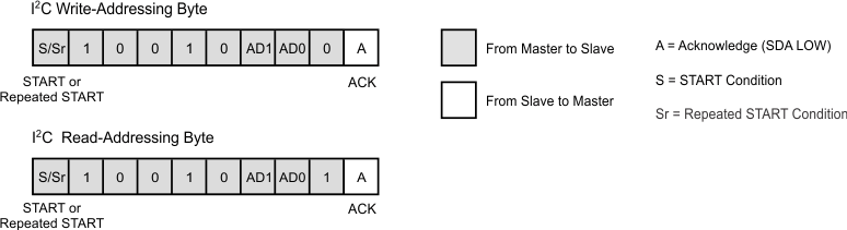 Figure 33. I2C Bus Addressing (Slave-Address Byte Format)
7.5.3 Control Byte
Table 6. Control Byte Format: Start a Conversion and Mode Setting, D7 = 1
| MSB D7 |
D6 | D5 | D4 | D3 | D2 | D1 | LSB D0 |
|---|---|---|---|---|---|---|---|
| 1
(Control Byte 1) |
C3 | C2 | C1 | C0 | RM | SWRST | STS |
| Control Byte ID (D7) |
1: Control Byte 1 (start conversion and channel select and conversion-related configuration). 0: Control Byte 0 (read/write data registers and non-conversion-related controls). |
| C[3:0] (D6:D3) |
Converter function select bits These bits select the input for conversion, and the converter function to be executed. Table 7 lists the possible converter functions. |
| RM (D2) |
Resolution select If RM = 1, the conversion-result resolution is 12-bit; otherwise, the resolution is 10-bit. This bit is the same RM bit shown in CFR0. 0: 10-bit 1: 12-bit |
| SWRST (D1) |
Software reset. This bit is self-clearing. 1: Reset all register values to default |
| STS (D0) |
Stop bit for all converter functions. This bit is self-clearing. On writing a 1 to this register, this bit aborts the converter function currently running in the TSC2013-Q1. An automatic write of 0 to this register occurs when the abort has completed. Setting this bit to 1 can only stop converter functions; it does not reset any data, status, or configuration registers. This bit is the same STS bit shown in CFR0, but reading can only be through the CFR0 register. Write 0: Normal operation Write 1: Stop converter functions and power down |
Table 7. Converter Function Select
| C3 | C2 | C1 | C0 | FUNCTION |
|---|---|---|---|---|
| 0 | 0 | 0 | 0 | Touch-Screen Scan function: X triplet, Y triplet, Z1, and Z2 coordinates converted and the results returned to X1, X2, IX, Y1, Y2, IY, Z1, and Z2 data registers. Scan continues until either lifting of the pen or sending of a stop bit. |
| 0 | 0 | 0 | 1 | Touch-Screen Scan function: IX and IY coordinates converted and the results returned to IX and IY data registers. Scan continues until either lifting of the pen or sending of a stop bit. |
| 0 | 0 | 1 | 0 | Touch screen function: X triplet converted and the results returned to X1, X2, IX data register. |
| 0 | 0 | 1 | 1 | Touch screen function: Y triplet converted and the results returned to Y1, Y2, IY data register. |
| 0 | 1 | 0 | 0 | Touch screen function: Z1 and Z2 coordinates converted and the results returned to Z1 and Z2 data registers. |
| 0 | 1 | 0 | 1 | Auxiliary input converted and the results returned to the AUX data register. |
| 0 | 1 | 1 | 0 | Touch screen function: IX converted and result returned to IX data register. |
| 0 | 1 | 1 | 1 | Touch screen function: IY converted and result returned to IY data register. |
| 1 | 0 | 0 | 0 | Auxiliary input conversion occurs continuously and the results returned to the AUX data register. |
| 1 | 0 | 0 | 1 | RESERVED |
| 1 | 0 | 1 | 0 | RESERVED |
| 1 | 0 | 1 | 1 | RESERVED(1) |
| 1 | 1 | 0 | 0 | RESERVED |
| 1 | 1 | 0 | 1 | X+, X– drivers activated |
| 1 | 1 | 1 | 0 | Y+, Y– drivers activated |
| 1 | 1 | 1 | 1 | Y+, X– drivers activated |
Table 8. Control Byte Format: Start a Conversion and Mode Setting D7 = 0
| MSB D7 |
D6 | D5 | D4 | D3 | D2 | D1 | LSB D0 |
|---|---|---|---|---|---|---|---|
| 0
(Control Byte 0) |
A3 | A2 | A1 | A0 | Reserved (Write 0) |
PND0 | R/W |
| Control byte ID (D7) |
1: Control byte 1—start conversion, channel select, and conversion-related configuration 0: Control byte 0—read/write data registers and non-conversion-related controls |
| A[3:0] (D6:D3) | Register address bits as detailed in Table 9 |
| RESERVED (D2) | Set a 0 in this bit for normal operation |
| PND0 (D1) |
Power-not-down control 1: ADC biasing circuitry is always on between conversions but shuts down after the converter function stops 0: ADC biasing circuitry shuts down either between conversions or after the converter function stops. Example power savings for the following condition is approximately 5%: AUX conversion, continuous mode, median filter = 15, averaging filter = 7, ƒ(ADC) = 2 MHz. |
| R/W (D0) |
TSC internal-register data-flow control 1: Set the starting address of the TSC internal registers for a register read (see Figure 34) 0: Write to TSC internal registers |
7.5.3.1 Touch-Screen Scan Function for XYZ or XY
These scan functions (C3–C0 = 0000 or 0001) can collaborate with the PSM bit that defines the control mode of converter functions. With the PSM bit set to 1, TI recommends issuing these scan-function select commands before detection of a pen touch in order to allow the TSC2013-Q1 device to initiate and control the scan processes immediately after detection of the screen touched. Without issuing these functions before detection of a pen touch, the TSC2013-Q1 waits for the host to write these functions before starting a scan process. If PSM stays as 1 after a TSC-initiated scan function is complete, the host is not required to write these function-select bits again for each of the following pen touches after the detected touch. In the host-controlled converter function mode (PSM = 0), the host must send these functions select bits repeatedly for each scan function after a detected pen touch.
NOTE
The update of the data registers may occur while a host reading is in progress. Using the sequential read cycle (see Figure 35) prevents the TSC from updating registers while a host reading is in progress. To ensure a correct reading of the XYZ or XY coordinates, use the sequential read cycle to read the coordinates after the scan.
Table 9. Internal Register Map
| REGISTER ADDRESS | |||||
|---|---|---|---|---|---|
| A3 | A2 | A1 | A0 | REGISTER CONTENT | READ/WRITE |
| 0 | 0 | 0 | 0 | X1 measurement result | R |
| 0 | 0 | 0 | 1 | X2 measurement result | R |
| 0 | 0 | 1 | 0 | Y1 measurement result | R |
| 0 | 0 | 1 | 1 | Y2 measurement result | R |
| 0 | 1 | 0 | 0 | IX measurement result | R |
| 0 | 1 | 0 | 1 | IY measurement result | R |
| 0 | 1 | 1 | 0 | Z1 measurement result | R |
| 0 | 1 | 1 | 1 | Z2 measurement result | R |
| 1 | 0 | 0 | 0 | Status | R |
| 1 | 0 | 0 | 1 | AUX measurement result | R |
| 1 | 0 | 1 | 0 | RESERVED | |
| 1 | 0 | 1 | 1 | RESERVED | |
| 1 | 1 | 0 | 0 | CFR0 | R/W |
| 1 | 1 | 0 | 1 | CFR1 | R/W |
| 1 | 1 | 1 | 0 | CFR2 | R/W |
| 1 | 1 | 1 | 1 | Converter function select status | R |
R/W is the register read and write control. A 1 indicates that the value of the internal register address bits A3–A0 is stored internally as the starting address for a register read (see Figure 34). The content of the addressed register is sent to SDA by using I2C read addressing (see Figure 35 and Figure 36). A0 indicates that the data following control byte 0 on SDA are written into the internal register addressed by bits A3–A0 (see Figure 34).
7.5.4 Start a Write Cycle
A write cycle begins when the master issues the slave address to the TSC2013-Q1 device. The slave address consists of seven address bits and a write bit (R/W = 0; see Table 6).On receipt of the eighth bit, if the address matches the AD1 through AD0 address input pin setting, the TSC2013-Q1 device issues an acknowledge bit by pulling SDA low for one additional clock cycle (ACK = 0); see Figure 33.
When the master receives the acknowledge bit from the TSC2013-Q1 device, the master writes the input control byte to the slave (see Table 6). After the control byte is received by the slave, the slave issues another acknowledge bit by pulling SDA low for one clock cycle (ACK = 0). The master then ends the write cycle by issuing a STOP or repeated START condition; see Figure 34.
7.5.5 Register Access
Data access begins with the master issuing a START (or repeated START) condition followed by the 7-bit address and a read bit (R/W = 1; see Table 6). On receipt of the eighth bit has been received and an address match, the slave issues an acknowledge by pulling SDA low for one clock cycle (ACK = 0). The first byte of serial data then follows. After the slave has sent the first byte, it then releases the SDA line for the master to issue an acknowledge (ACK = 0). The slave issues the second byte of serial data on receiving the acknowledgment from the master (D7–D0), followed by a not-acknowledge bit (ACK = 1) from the master to indicate receipt of the last data byte has been received. The master then issues a STOP condition (P) or repeated START (Sr), which ends the read cycle, as shown in Figure 35 and Figure 36. If the master issues a not-acknowledge (ACK = 1) after receipt of the first data byte, the master must then issue a stop condition (P) to reset the registers. If the master is not ready to receive the second data byte, it should issue the acknowledge (ACK = 0), or the master should stretch the clock. On restart of the clock, the master can receive the second byte of data.
7.5.6 Communication Protocol
All control of the TSC2013-Q1 is through registers. Reading and writing to these registers are accomplished by the use of Control Byte 0, which includes a 4-bit address plus one read-write TSC register-control bit. The data registers defined in Table 9 are all 16-bit, right-adjusted.
NOTE
Except for some configuration registers and the status register that are full 16-bit registers, the rest of the value registers are 12-bit (or 10-bit) data preceded by four (or six) zeros.
See the Configuration and Status Registers section for the register field descriptions.
7.5.7 Register Reset
The TSC2013-Q1 device can be reset in one of three ways. First, at power-on, a power-good signal generates a prolonged reset pulse internally to all registers.
Second, an external pin, RESET, is available to perform a system reset or allow other peripherals (such as a display) to reset the device if the pulse meets the timing requirement (at least 10 μs in duration). Any RESET pulse less than 5 μs is rejected. To accommodate the timing drift between devices because of process variation, a RESET pulse duration between 5 μs and 10 μs falls into the gray area that is unrecognized, giving an undetermined result; avoid this situation. See Figure 37 for details. A good reset pulse must be low for at least 10 μs. An internal spike filter is available to reject spikes up to 20 ns wide.
Third, a software reset is activated by writing a 1 to CB1.1 (bit 1 of control byte 1). Note that this reset is not self-clearing, so the user must write a 0 to remove the software reset.
A reset clears all registers and loads default values. A power-on reset and external (hardware) reset take precedence over a software reset. If the user does not clear a software reset, either a power-on reset or an external (hardware) reset clears it.
7.6 Register Maps
The TSC2013-Q1 device has several 16-bit registers that allow control of the device, as well as providing a location to store results from the TSC2013-Q1 device until read out by the host microprocessor. Table 10 shows the memory map.
Table 10. Register Content and Reset Values(1)
| A3-A0 (HEX) |
REGISTER NAME |
D15 | D14 | D13 | D12 | D11 | D10 | D9 | D8 | D7 | D6 | D5 | D4 | D3 | D2 | D1 | D0 | RESET VALUE (HEX) |
|---|---|---|---|---|---|---|---|---|---|---|---|---|---|---|---|---|---|---|
| 0 | X1 | 0 | 0 | 0 | 0 | R11 | R10 | R9 | R8 | R7 | R6 | R5 | R4 | R3 | R2 | R1 | R0 | 0000 |
| 1 | X2 | 0 | 0 | 0 | 0 | R11 | R10 | R9 | R8 | R7 | R6 | R5 | R4 | R3 | R2 | R1 | R0 | 0000 |
| 2 | Y1 | 0 | 0 | 0 | 0 | R11 | R10 | R9 | R8 | R7 | R6 | R5 | R4 | R3 | R2 | R1 | R0 | 0000 |
| 3 | Y2 | 0 | 0 | 0 | 0 | R11 | R10 | R9 | R8 | R7 | R6 | R5 | R4 | R3 | R2 | R1 | R0 | 0000 |
| 4 | IX | T(2) | 0 | 0 | 0 | R11 | R10 | R9 | R8 | R7 | R6 | R5 | R4 | R3 | R2 | R1 | R0 | 0000 |
| 5 | IY | T(2) | 0 | 0 | 0 | R11 | R10 | R9 | R8 | R7 | R6 | R5 | R4 | R3 | R2 | R1 | R0 | 0000 |
| 6 | Z1 | 0 | 0 | 0 | 0 | R11 | R10 | R9 | R8 | R7 | R6 | R5 | R4 | R3 | R2 | R1 | R0 | 0000 |
| 7 | Z2 | 0 | 0 | 0 | 0 | R11 | R10 | R9 | R8 | R7 | R6 | R5 | R4 | R3 | R2 | R1 | R0 | 0000 |
| 8 | Status | DAVX | DAVY | DAVZ1 | DAVZ2 | DAVAUX | 0 | 0 | 0 | RESET | 0 | 0 | 0 | 0 | PDST | 0 | 0 | 0004 |
| 9 | AUX | 0 | 0 | 0 | 0 | R11 | R10 | R9 | R8 | R7 | R6 | R5 | R4 | R3 | R2 | R1 | R0 | 0000 |
| A | RSVD | 0 | 0 | 0 | 0 | 0 | 0 | 0 | 0 | 0 | 0 | 0 | 0 | 0 | 0 | 0 | 0 | 0000 |
| B | RSVD | 0 | 0 | 0 | 0 | 0 | 0 | 0 | 0 | 0 | 0 | 0 | 0 | 0 | 0 | 0 | 0 | 0000 |
| C | CFR0 | PSM | STS | RM | CL1 | CL0 | PV2 | PV1 | PV0 | PR2 | PR1 | PR0 | SN2 | SN1 | SN0 | DTW | LSM | 4000 |
| D | CFR1 | 0 | 0 | 0 | 0 | 0 | 0 | 0 | 0 | 0 | 0 | 0 | 0 | 0 | BTD2 | BTD1 | BTD0 | 0000 |
| E | CFR2 | PINTS1 | PINTS0 | M1 | M0 | W1 | W0 | 0 | 0 | 0 | 0 | 0 | MAVE X TRIPLET |
MAVE Y TRIPLET |
MAVE Z |
MAVE AUX |
0 | 0000 |
| F | CFN | CFN15 | CFN14 | CFN13 | 0 | 0 | 0 | 0 | CFN8 | CFN7 | R6 | R5 | R4 | R3 | R2 | R1 | R0 | 0000 |
T = 0: No touch detected during conversion
T = 1: Touch detected during conversion
7.6.1 Configuration and Status Registers
7.6.1.1 Configuration Register 0
7.6.1.1.1 Configuration Register 0 (address = 0) [reset = 4000h for read; 0000h for write]
| D15 | D14 | D13 | D12 | D11 | D10 | D9 | D8 |
| PSM | STS | RM | CL[1:0] | PV[2:0] | |||
| R/W-Reset | R/W- | R/W- | R/W- | R/W- | |||
| D7 | D6 | D5 | D4 | D3 | D2 | D1 | D0 |
| PR[2:0] | SN[2:0] | DTW | LSM | ||||
| R/W- | R/W- | R/W- | R/W- | ||||
Table 11. Configuration Register 0 Field Descriptions
| Bit | Field | Type | Reset | Description |
|---|---|---|---|---|
| D15 | PSM | R/W | 0 |
Pen status or control mode. This bit is the MSB. Reading this bit allows the host to determine if a touch of the screen has occurred. Writing to this bit selects the mode used to control the flow of converter functions that are either initiated and/or controlled by host or under control of the TSC2013-Q1 responding to a pen touch. When reading, the PSM bit indicates if the pen is down or not. When writing to this register, this bit determines if the TSC2013-Q1 or the host controls the converter functions. The default state is the host-controlled converter function mode (0). The other state (1) is the TSC-initiated scan function mode that must only collaborate with C3–C0 = 0000 or 0001 in order to allow the TSC2013-Q1 to initiate and control the scan function for XYZ or XY when a on detection of a pen touch.
0 (R): No screen touch detected 1 (R): Screen touch detected 0 (W): Converter functions initiated and/or controlled by host 1 (W): Converter functions initiated and controlled by the TSC2013-Q1 |
| D14 | STS | R/W | 1 for R 0 for W |
ADC status When reading, this bit indicates if the converter is busy or not busy. Continuous scans or conversions can be stopped by writing a 1 to this bit, immediately aborting the running converter function (even if the pen is still down) and causing the ADC to power down. The default state for write is 0 (normal operation), and the default state for read is 1 (converter is not busy). Note that the same bit can be written through Control Byte 1 (bit 0). This bit is self-clearing.
0 (R): Converter is busy 1 (R): Converter is not busy 0 (W): Normal operation 1 (W): Stop converter function and power down |
| D13 | RM | R/W | 0 |
Resolution control This bit specifies the ADC resolution. See for a description of these bits. This bit is the same whether reading or writing, and defaults to 0. Note that one cn write the same bit through Control Byte 1.
0: 10-bit resolution. Default after power up and reset 1: 12-bit resolution |
| D12-D11 | CL[1:0] | R/W | 0 |
Conversion-clock control These two bits specify CL bits that specify the clock rate that the ADC uses to perform conversion. CL1 = 0, CL0 = 0: ƒ(ADC) = ƒ(OSC) / 1, referred to as the 4-MHz ADC clock rate, 10-bit resolution only CL1 = 0, CL0 = 1: ƒ(ADC) = ƒ(OSC) / 2, referred to as the 2-MHz ADC clock rate CL1 = 1, CL0 = 0: ƒ(ADC) = ƒ(OSC) / 4, referred to as the 1-MHz ADC clock rate CL1 = 1, CL0 = 1: ƒ(ADC) = ƒ(OSC) / 4, referred to as the 1-MHz ADC clock rate |
| D10-D8 | PV[2:0] | R/W | 0 |
Panel-voltage stabilization-time control These bits specify a delay time from the moment of touch-screen drivers enabling to the time of voltage sampling and the start of a conversion. These bits allow the user to adjust the appropriate settling time for the touch panel and external capacitances. See for settings of these bits. The default state is 000, indicating a 0-μs stabilization time (t(PVS)). These bits are the same whether reading or writing. PV2 = 0, PV1 = 0, PV0 = 0: 0 μs PV2 = 0, PV1 = 0, PV0 = 1: 100 μs PV2 = 0, PV1 = 1, PV0 = 0: 500 μs PV2 = 0, PV1 = 1, PV0 = 1: 1 ms PV2 = 1, PV1 = 0, PV0 = 0: 5 ms PV2 = 1, PV1 = 0, PV0 = 1: 10 ms PV2 = 1, PV1 = 1, PV0 = 0: 50 ms PV2 = 1, PV1 = 1, PV0 = 1: 100 ms |
| D7-D5 | PR[2:0] | R/W | 0 |
Precharge time selection These bits set the amount of time allowed for precharging any pin capacitance on the touch screen prior to sensing whether a pen touch is in progress. The following lists the precharge time (t(PRE)) PR2 = 0, PR1 = 0, PR0 = 0: 20 μs PR2 = 0, PR1 = 0, PR0 = 1: 84 μs PR2 = 0, PR1 = 1, PR0 = 0: 276 μs PR2 = 0, PR1 = 1, PR0 = 1: 340 μs PR2 = 1, PR1 = 0, PR0 = 0: 1.044 ms PR2 = 1, PR1 = 0, PR0 = 1: 1.108 ms PR2 = 1, PR1 = 1, PR0 = 0: 1.3 ms PR2 = 1, PR1 = 1, PR0 = 1: 1.364 ms |
| D4-D2 | SN[2:0] | R/W | 0 |
Sense-time selection These bits set the amount of time the TSC2013-Q1 device waits after converting a coordinate to sense whether a screen touched is in progress. SNS2 = 0, SNS1 = 0, SNS0 = 0: 32 μs SNS2 = 0, SNS1 = 0, SNS0 = 1: 96 μs SNS2 = 0, SNS1 = 1, SNS0 = 0: 544 μs SNS2 = 0, SNS1 = 1, SNS0 = 1: 608 μs SNS2 = 1, SNS1 = 0, SNS0 = 0: 2.08 ms SNS2 = 1, SNS1 = 0, SNS0 = 1: 2.144 ms SNS2 = 1, SNS1 = 1, SNS0 = 0: 2.592 ms SNS2 = 1, SNS1 = 1, SNS0 = 1: 2.656 ms |
| D1 | DTW | R/W | 0 |
Detection of pen touch in wait (patent pending) Writing a 1 to this bit enables pen-touch detection in the background while waiting for the host to issue the converter function in host-initiated and -controlled modes. This background detection allows the TSC2013-Q1 to pull PINTDAV high to indicate no pen touch detected while waiting for the host to issue the converter function. If the host polls a high state at PINTDAV before the transmission of the convert function, the host can abort the issuance of the convert function and stay in the polling PINTDAV mode until the detection of the next pen touch. |
| D0 | LSM | R/W | 0 |
Longer sampling mode. This bit is the LSB. With this bit set to 1, an extra 500 ns of sampling time is added to the normal sampling cycles of each conversion. This additional time is represented as approximately two internal oscillator clock cycles. |
7.6.1.2 Configuration Register 1 (address = Dh) [reset = 0000h]
Configuration register 1 (CFR1) defines the connection test-bit modes configuration and batch-delay selection.
| D15 | D14 | D13 | D12 | D11 | D10 | D9 | D8 |
| RESERVED | |||||||
| W-0 | |||||||
| D7 | D6 | D5 | D4 | D3 | D2 | D1 | D0 |
| RESERVED | BTD[2:0] | ||||||
| W-0 | R/W-0 | ||||||
Table 12. Configuration Register 1 Field Descriptions
| Bit | Field | Type | Reset | Description |
|---|---|---|---|---|
| D15-D3 | RESERVED | W | 0 | |
| D2-D0 | BTD[2:0] | R/W | 0 |
Batch time-delay mode These are the selection bits that specify the delay before the triggering of a sample or conversion scan cycle. When it is set, Batch time-delay mode uses a set of timers to trigger a sequence of sample-and-conversion events automatically. The mode works for both TSC-initiated scans (XYZ or XY) and host-initiated scans (XYZ or XY). Configure a TSC-initiated scan (XYZ or XY) by setting the PSM bit in CFR0 to 1 and C[3:0] in control byte 1 to 0000 or 0001. In the case of a TSC-initiated scan (XYZ or XY), the sequence begins with the TSC responding to a pen touch. After the first processed sample set completes during the batch delay, the scan enters a wait mode until the end of the batch delay. If detection of a pen touch persists at that moment, the scan continues to process the next sample set, along with a resumption of the batch delay. The selected batch delay during the time of the detected pen touch regulates the throughput of the processed sample sets (shown in as sample sets per second, or SSPS). One can configure a TSC-initiated scan (XYZ or XY) by setting the PSM bit in CFR0 to 1 and C[3:0] in control byte 1 to 0000 or 0001. Note that the throughput of the processed sample set also depends on the settings of stabilization, precharge, and sense times, and the total number of samples to be processed per coordinates. If the accrual time of these factors exceeds the batch delay time, the accrual time dominates. Batch delay time starts when the pen touch initiates the scan function that converts coordinates. One can configure a host-initiated scan (XYZ or XY) by setting the PSM bit in CFR0 to 0 and C[3:0] in control byte 1 to 0000 or 0001. For the host-initiated scan (XYZ or XY), the host must set TSC internal register C[3:0] in control byte 1 to 0000 or 0001 initially after a pen-touch detection; see . After engagement of the scan (XYZ or XY), the selected batch-delay timer regulates the throughput of the processed sample sets, as long as the initial detected touch is uninterrupted. |
|
Throughput for TSC-initiated or host-initiated scan, XYZ OR XY: BTD2 = 0, BTD1 = 0, BTD0 = 0, td = 0: Normal operation throughput depends on settings BTD2 = 0, BTD1 = 0, BTD0 = 1, td = 1: 1000 SSPS BTD2 = 0, BTD1 = 1, BTD0 = 0, td = 2: 500 SSPS BTD2 = 0, BTD1 = 1, BTD0 = 1, td = 4: 250 SSPS BTD2 = 1, BTD1 = 0, BTD0 = 0, td = 10: 100 SSPS BTD2 = 1, BTD1 = 0, BTD0 = 1, td = 20: 50 SSPS BTD2 = 1, BTD1 = 1, BTD0 = 0, td = 40: 25 SSPS BTD2 = 1, BTD1 = 1, BTD0 = 1, td = 100: 10 SSPS For example, if stabilization time, precharge time, and sense time are selected as 100 μs, 84 μs, and 96 μs, respectively, and the batch delay time is 2 ms, then the scan function enters wait mode after the first processed sample set until the 2 ms of batch-delay time expires. When the scan function starts to process the second sample set (if a touch is still present on the screen), the batch delay restarts at 2 ms (in this example). This procedure remains regulated by 2 ms until the pen touch is undetected or a stop bit or any reset form stops the scan function. |
7.6.1.3 Configuration Register 2 (address = Eh) [reset = 0000h]
Configuration register 2 (CFR2) defines the preprocessor configuration.
| D15 | D14 | D13 | D12 | D11 | D10 | D9 | D8 |
| PINTS1 | PINTS0 | M[1:0] | W[1:0] | RESERVED | |||
| R/W-0 | R/W-0 | R/W-00 | R/W-00 | W-0 | |||
| D7 | D6 | D5 | D4 | D3 | D2 | D1 | D0 |
| RESERVED | MAVE X TRIPLET |
MAVE Y TRIPLET |
MAVE Z |
MAVE AUX |
RESERVED | ||
| W-0 | R/W-0000 | R/W-0000 | R/W-0000 | R/W-0000 | W-0 | ||
Table 13. Configuration Register 2 Field Descriptions
| Bit | Field | Type | Reset | Description |
|---|---|---|---|---|
| D15 | PINTS1 | R/W | 0 |
This bit controls the output format of the PINTDAV pin. With this bit set to 0, the output format is the AND-form of internal signals of PENIRQ and DAV). With this bit set to 1, PINTDAV outputs PENIRQ only. PINTDAV PIN OUTPUT = 0: AND combination of PENIRQ (active-low) and DAV (active-high). 0: Data available, DAV (active-low). 1: Interrupt, PENIRQ (active-low) generated by pen-touch. 1: Data available, DAV (active-low). |
| D14 | PINTS0 | R/W | 0 |
This bit selects the output on the PINTDAV pin. With this bit set to 0, the output format of PINTDAV depends on the selection made on the PINTS1 bit. With this bit set to 1, PINTDAV outputs the internal signal of DAV. PINTDAV PIN OUTPUT = 0: AND combination of PENIRQ (active-low) and DAV (active-high). 1: Data available, DAV (active-low). 0: Interrupt, PENIRQ (active-low) generated by pen-touch. 1: Data available, DAV (active-low). |
| D13-D12 | M[1:0] | R/W | 00 |
Preprocessing MAV filter control Note that when the MAV filter is processing data, the STS bit and the corresponding DAV bits in the status register indicate that the converter is busy until all conversions necessary for the preprocessing are complete. The default state for these bits is 0000, which bypasses the preprocessor. These bits are the same whether reading or writing. |
| D11-D10 | W[1:0] | R/W | 00 |
Preprocessing MAV filter control Note that when the MAV filter is processing data, the STS bit and the corresponding DAV bits in the status register indicate that the converter is busy until all conversions necessary for the preprocessing are complete. The default state for these bits is 0000, which bypasses the preprocessor. These bits are the same whether reading or writing. |
| D9-D5 | RESERVED | W | 0 | |
| D4-D1 | MAVE | R/W | 0000 |
MAV-filter function-enable bit When any bit is set to 1, the MAV filter setup is applied to the corresponding measurement. |
| D0 | RESERVED | W | 0 |
7.6.1.4 Converter-Function Select Register (address = Fh) [reset = 0000h]
The converter-function select (CFN) register reflects the converter function select status.
| D15 | D14 | D13 | D12 | D11 | D10 | D9 | D8 |
| CFN[15:13] | RESERVED | CFN[8:0] | |||||
| R-0 | R-0 | R-0 | |||||
| D7 | D6 | D5 | D4 | D3 | D2 | D1 | D0 |
| CFN[8:0] | |||||||
| R-0 | |||||||
Table 14. Converter-Function Select Register Field Descriptions
| Bit | Field | Type | Reset | Description |
|---|---|---|---|---|
| D15-D13 | CFN[15:13] | R | 0 |
Touch-screen driver status These bits represent the current status of the turned-on touch-screen drivers. The device sets CFN13 to 1 with both X+ and X– drivers turned on, CFN14 to 1 with both Y+ and Y– drivers turned on, and CFN15 to 1 with Y+ and X– drivers turned on. Otherwise, the device sets these bits to 0. The device resets these bits to 000b whenever the converter function is complete, stopped by the STS bit, or reset (by a hardware reset from the RESET pin or a software reset from SWRST bit in control byte 1). |
| D12-D9 | RESERVED | R | 0 | |
| D8-D0 | CFN[8:0] | R | 0 |
Converter function-select status. These bits represent the converter function currently running, which is set in bits C3–C0 of control byte 1. When the CFNx bit shows 1, where x is the decimal value of converter function-select bits C3–C0, it is an indication that the converter function set in bits C3–C0 is running. For example, when CFN2 shows 1, it indicates the converter function set in bits C3-C0 (0010) is running. Reset of the CFNx bits to 0000h occurs whenever the converter function is complete, stopped by STS bit, or reset (by the hardware reset from the RESET pin or the software reset from SWRST bit in Control Byte 1). However, if the TSC sets the PSM bit in the CFR0 register to 1 to initiate the scan-function mode, reset of the CFN0 or CFN1 does not occur when the corresponding converter function is complete, because there is no pen touch. This event allows the TSC2013-Q1 to initiate the scan process (corresponding to CFN0 or CFN1 set to 1) immediately on detection of the next pen touch. |
7.6.1.5 Status Register (address = 8h) [reset = 0004h]
The Status Register provides information about the TSC2013-Q1 status.
| D15 | D14 | D13 | D12 | D11 | D10 | D9 | D8 |
| DAV Due X TRIPLET |
DAV Due Y TRIPLET |
DAV Due Z1 |
DAV Due Z2 |
DAV Due AUX |
RESERVED | ||
| R-0 | R-0 | ||||||
| D7 | D6 | D5 | D4 | D3 | D2 | D1 | D0 |
| RESET Flag |
RESERVED | PDST | RESERVED | ||||
| R-0 | R-0 | R-1 | R-0 | ||||
Table 15. Status Register Field Descriptions
| Bit | Field | Type | Reset | Description |
|---|---|---|---|---|
| D15-D11 | DAV | R | 0 |
Data available bits These five bits mirror the operation of the internal signals of DAV. On storing any processed data in data registers, the DAV bit (D15 to D11) corresponding to the data type is set to 1. The bIt stays at 1 until the registers updated to the host has read out the processed data. If the user submits a single IX or single IY conversion command, bit D15 or D14 (respectively) shows data availability. In this case, only data register IX or IY receives an update. 0: No new processed data are available. 1: Processed data are available. This bit remains at 1 until the host has read out all updated registers. |
| D10-D8 | RESERVED | R | 0 | |
| D7 | RESET | R | 0 |
Interpretation of the RESET flag bits: 0: Device was reset since the last status poll (hardware or software reset). 1: Device reset has not occurred since the last status poll. |
| D6-D3 | RESERVED | R | 0 | |
| D2 | PDST | R | 1 |
Power-down status This bit reflects the setting of the PND0 bit in Control Byte 0. When this bit shows 0, it indicates ADC bias circuitry power is still on after each conversion and before the next sampling; otherwise, it indicates ADC bias circuitry power is down after each conversion and before the next sampling. However, power is down between conversion sets. Because this status bit is in synchrony with the internal clock, it does not reflect the setting of the PND0 bit until detection of a pen touch is detected or initiation of a converter function. |
| D1-D0 | RESERVED | R | 0 |
7.6.2 Data Registers
The data registers of the TSC2013-Q1 hold data results from conversions. All of these registers default to 0000h on reset.
7.6.2.1 X1, X2, IX, Y1, Y2, IY, Z1, Z2, and AUX registers (offset = see Table 10) [reset = see Table 10]
The results of all ADC conversions are placed in the appropriate data registers, as described in Table 9. The data format of the result word (R) of these registers is right-justified, as shown in .
| D15 | D14 | D13 | D12 | D11 | D10 | D9 | D8 |
| RESERVED | R11(1) | R10(1) | R9 | R8 | |||
| R-0 | R-0 | R-0 | R-0 | R-0 | |||
| D7 | D6 | D5 | D4 | D3 | D2 | D1 | D0 |
| R7 | R6 | R5 | R4 | R3 | R2 | R1 | R0 |
| R-0 | R-0 | R-0 | R-0 | R-0 | R-0 | R-0 | R-0 |
Table 16. X1, X2, IX, Y1, Y2, IY, Z1, Z2, and AUX Register Field Descriptions
| Bit | Field | Type | Reset | Description |
|---|---|---|---|---|
| D15-D12 | RESERVED | R | 0 | Use of the D15 bit only occurs during a single IX or single IY conversion command (see Table 10). T = 0: No touch detected during conversion T = 1: Touch detected during conversion |
| D11-D0 | R[11:0] | R | 0 | 12-bit data |