ZHCSCV1A June   2014  – July 2014 TSC2013-Q1

PRODUCTION DATA.  

  1. 特性
  2. 应用
  3. 说明
  4. 修订历史记录
  5. Pin Configurations and Functions
  6. Specifications
    1. 6.1  Absolute Maximum Ratings
    2. 6.2  Handling Ratings
    3. 6.3  Recommended Operating Conditions
    4. 6.4  Thermal Information
    5. 6.5  Electrical Characteristics
    6. 6.6  Timing Requirements — I2C Standard Mode (ƒ(SCL) = 100 kHz)
    7. 6.7  Timing Requirements — I2C Fast Mode (ƒ(SCL) = 400 kHz)
    8. 6.8  Timing Requirements — I2C High-Speed Mode (ƒ(SCL) = 1.7 MHz)
    9. 6.9  Timing Requirements — I2C High-Speed Mode (ƒ(SCL) = 3.4 MHz)
    10. 6.10 Typical Characteristics
  7. Detailed Description
    1. 7.1 Overview
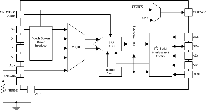
    2. 7.2 Functional Block Diagram
    3. 7.3 Feature Description
      1. 7.3.1 Touch-Screen Operation
      2. 7.3.2 4-Wire Touch Screen Measurements
      3. 7.3.3 Analog-to-Digital Converter
        1. 7.3.3.1 Data Format
        2. 7.3.3.2 Reference
        3. 7.3.3.3 Variable Resolution
        4. 7.3.3.4 Conversion Clock and Conversion Time
        5. 7.3.3.5 Touch Detect
        6. 7.3.3.6 Preprocessing
          1. 7.3.3.6.1 Preprocessing—Median Value Filter and Averaging Value Filter
    4. 7.4 Device Functional Modes
      1. 7.4.1 Conversion Controlled by TSC2013-Q1 and Initiated by TSC2013-Q1 (TSMode 1)
        1. 7.4.1.1 IX-IY Scan
        2. 7.4.1.2 X-Triplet, Y-Triplet, Z-Scan
      2. 7.4.2 Conversion Controlled by TSC2013-Q1 and Initiated by Host (TSMode 2)
      3. 7.4.3 Conversion Controlled by Host (TSMode 3)
    5. 7.5 Programming
      1. 7.5.1 I2C Interface
        1. 7.5.1.1 I2C Fast or Standard Mode (F-S Mode)
        2. 7.5.1.2 I2C High-Speed Mode (Hs Mode)
      2. 7.5.2 Digital Interface
        1. 7.5.2.1 Address Byte
      3. 7.5.3 Control Byte
        1. 7.5.3.1 Touch-Screen Scan Function for XYZ or XY
      4. 7.5.4 Start a Write Cycle
      5. 7.5.5 Register Access
      6. 7.5.6 Communication Protocol
      7. 7.5.7 Register Reset
    6. 7.6 Register Maps
      1. 7.6.1 Configuration and Status Registers
        1. 7.6.1.1 Configuration Register 0
          1. 7.6.1.1.1 Configuration Register 0 (address = 0) [reset = 4000h for read; 0000h for write]
        2. 7.6.1.2 Configuration Register 1 (address = Dh) [reset = 0000h]
        3. 7.6.1.3 Configuration Register 2 (address = Eh) [reset = 0000h]
        4. 7.6.1.4 Converter-Function Select Register (address = Fh) [reset = 0000h]
        5. 7.6.1.5 Status Register (address = 8h) [reset = 0004h]
      2. 7.6.2 Data Registers
        1. 7.6.2.1 X1, X2, IX, Y1, Y2, IY, Z1, Z2, and AUX registers (offset = see ) [reset = see ]
  8. Application and Implementation
    1. 8.1 Application Information
      1. 8.1.1 Auxiliary Measurement
      2. 8.1.2 Single IX or Single IY Measurement
    2. 8.2 Typical Application
      1. 8.2.1 Design Requirements
      2. 8.2.2 Detailed Design Procedure
        1. 8.2.2.1 Power-On-Reset and Reset Consideration
          1. 8.2.2.1.1 Power-On Reset
          2. 8.2.2.1.2 Requesting a Minimal t(SNSVDD_OFF) Time
          3. 8.2.2.1.3 Requesting a Minimal t(SNSVDD_OFF_ramp) and t(SNSVDD_ON_ramp) Ramp
          4. 8.2.2.1.4 Hardware Reset
          5. 8.2.2.1.5 Software Reset
        2. 8.2.2.2 Power Up Considerations
          1. 8.2.2.2.1 Power-Off Cycles During Normal Operation
          2. 8.2.2.2.2 Supply Glitches During Normal Operation
          3. 8.2.2.2.3 TSC2013-Q1 Digital Pins
          4. 8.2.2.2.4 Suggested Hardware Reset During Power-On
        3. 8.2.2.3 Device Timing Setup and Use
          1. 8.2.2.3.1 Touch-Panel Driving Power
          2. 8.2.2.3.2 ADC Clock Effects
        4. 8.2.2.4 Panel Voltage Stabilization Time
        5. 8.2.2.5 Precharge and Sense Time
        6. 8.2.2.6 Single-Touch Operation
      3. 8.2.3 Application Curves
  9. Power Supply Recommendations
  10. 10Layout
    1. 10.1 Layout Guidelines
    2. 10.2 Layout Example
  11. 11器件和文档支持
    1. 11.1 商标
    2. 11.2 静电放电警告
    3. 11.3 术语表
  12. 12机械封装和可订购信息

封装选项

机械数据 (封装 | 引脚)
散热焊盘机械数据 (封装 | 引脚)
订购信息

1 特性

  • 符合汽车应用要求
  • 具有符合 AEC-Q100 的下列结果:
    • 器件温度 1 级:-40°C 至 125°C 的
    • 器件人体模型 (HBM) 静电放电 (ESD) 分类等级 2
    • 器件充电器件模型 (CDM) ESD 分类等级 C4B
  • 4 线制触摸屏界面
  • 比例换算
  • 1.6V 至 3.6V 单电源:
    • I/OVDD 1.2V 至 3.6V
    • SNSVDD:1.6V 至 3.6V
  • 通过预处理减少总线活动
  • 高速 I2C 兼容接口
  • 屏幕触摸内部检测
  • 基于寄存器可编程:
    • 10 位或 12 位分辨率
    • 采样速率
    • 系统时序
  • 触摸压力测量
  • 自动断电控制
  • 低功耗:
    • 1.8V,50SSPS 时为 430μA
    • 1.6V,50SSPS 时为 320μA
    • 1.6V,8.2kSPS(设备采样率) 时为 58μA

2 应用

  • 汽车信息娱乐显示屏
  • 汽车导航系统
  • 工业用户界面
  • 医疗设备
  • 消费类便携电子产品

3 说明

TSC2013-Q1 器件是一款超低功耗双触摸屏控制器,设计用于搭配汽车信息娱乐和导航系统中的功耗敏感型低成本触摸显示屏使用。 其具有完整的超低功耗 12 位模数转换 (ADC) 电阻式触摸屏转换器,包括驱动器和测量触摸压力的控制逻辑。

TSC2013-Q1 器件可通过标准四线制界面实现捏拉缩放和旋转功能。 针对所有三种定义模式(标准、快速与高速),该器件均支持 I2C 串行总线与数据传输协议。 可轻松对 10 或 12 位范围内的 ADC 进行编程,以实现对系统和用户体验的自定义。

器件信息(1)

部件号 封装 封装尺寸(标称值)
TSC2013-Q1 PVQFN (16) 4.00mm x 4.00mm
TSSOP (16) 4.40mm × 5.00mm
(1) 要了解所有可用封装,请见数据表末尾的可订购产品附录。

方框图

fbd_slvsc89.gif