SCES707C August   2008  – December 2016 TS5A12301E

PRODUCTION DATA.  

  1. Features
  2. Applications
  3. Description
  4. Revision History
  5. Pin Configuration and Functions
  6. Specifications
    1. 6.1 Absolute Maximum Ratings
    2. 6.2 ESD Ratings
    3. 6.3 Recommended Operating Conditions
    4. 6.4 Thermal Information
    5. 6.5 Electrical Characteristics - 5-V Supply
    6. 6.6 Electrical Characteristics - 3.3-V Supply
    7. 6.7 Electrical Characteristics - 2.5-V Supply
    8. 6.8 Typical Characteristics
  7. Parameter Measurement Information
  8. Detailed Description
    1. 8.1 Overview
    2. 8.2 Functional Block Diagram
    3. 8.3 Feature Description
      1. 8.3.1 Isolation
      2. 8.3.2 1.8-V Compatible Logic
      3. 8.3.3 Integrated Control Input Pulldown
    4. 8.4 Device Functional Modes
  9. Application and Implementation
    1. 9.1 Application Information
    2. 9.2 Typical Application
      1. 9.2.1 Design Requirements
      2. 9.2.2 Detailed Design Procedure
      3. 9.2.3 Application Curve
  10. 10Power Supply Recommendations
  11. 11Layout
    1. 11.1 Layout Guidelines
    2. 11.2 Layout Example
  12. 12Device and Documentation Support
    1. 12.1 Receiving Notification of Documentation Updates
    2. 12.2 Community Resources
    3. 12.3 Trademarks
    4. 12.4 Electrostatic Discharge Caution
    5. 12.5 Glossary
  13. 13Mechanical, Packaging, and Orderable Information

封装选项

机械数据 (封装 | 引脚)
散热焊盘机械数据 (封装 | 引脚)
订购信息

Pin Configuration and Functions

YFP Package
6-Pin DSBGA
Top View
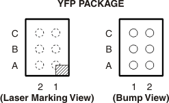
TS5A12301E po_ces707.gif

Pin Functions

PIN I/O DESCRIPTION
NAME NO.
COM B2 I/O Common signal path
GND B1 Ground
IN A2 I Digital control:
High = COM connected to NO
Low = COM connected to NC
Floating = COM connected to NC
NC C1 I/O Normally closed signal path
NO A1 I/O Normally open signal path
VCC C2 Power supply