SCDS225B March 2007 – January 2015 TS3A44159
PRODUCTION DATA.
- 1 Features
- 2 Applications
- 3 Description
- 4 Revision History
- 5 Pin Configuration and Functions
-
6 Specifications
- 6.1 Absolute Maximum Ratings
- 6.2 ESD Ratings
- 6.3 Recommended Operating Conditions
- 6.4 Thermal Information
- 6.5 Electrical Characteristics for 1.8-V Supply
- 6.6 Electrical Characteristics for 2.1-V Supply
- 6.7 Electrical Characteristics for 2.5-V Supply
- 6.8 Electrical Characteristics for 3.3-V Supply
- 6.9 Electrical Characteristics for 4.3-V Supply
- 6.10 Typical Characteristics
- 7 Parameter Measurement Information
- 8 Detailed Description
- 9 Application and Implementation
- 10Power Supply Recommendations
- 11Layout
- 12Device and Documentation Support
- 13Mechanical, Packaging, and Orderable Information
封装选项
请参考 PDF 数据表获取器件具体的封装图。
机械数据 (封装 | 引脚)
- PW|16
- RGT|16
- RSV|16
散热焊盘机械数据 (封装 | 引脚)
订购信息
6 Specifications
6.1 Absolute Maximum Ratings
over operating free-air temperature range (unless otherwise noted)(1)(2)| MIN | MAX | UNIT | |||
|---|---|---|---|---|---|
| VCC | Supply voltage(3) | –0.5 | 4.6 | V | |
| VNC
VNO VCOM |
Analog voltage(3)(4)(5) | –0.5 | VCC + 0.5 | V | |
| IK | Analog port diode current | VNC, VNO, VCOM < 0 | –50 | mA | |
| INC
INO ICOM |
ON-state switch current | VNC, VNO, VCOM = 0 to VCC | –200 | 200 | mA |
| ON-state peak switch current(6) | –400 | 400 | |||
| VIN | Digital input voltage | –0.5 | 4.6 | V | |
| IIK | Digital input clamp current(3)(4) | VI < 0 | –50 | mA | |
| ICC | Continuous current through VCC | 100 | mA | ||
| IGND | Continuous current through GND | –100 | mA | ||
| Tstg | Storage temperature | –65 | 150 | °C | |
(1) Stresses beyond those listed under Absolute Maximum Ratings may cause permanent damage to the device. These are stress ratings only, which do not imply functional operation of the device at these or any other conditions beyond those indicated under Recommended Operating Conditions. Exposure to absolute-maximum-rated conditions for extended periods may affect device reliability.
(2) The algebraic convention, whereby the most negative value is a minimum and the most positive value is a maximum
(3) All voltages are with respect to ground, unless otherwise specified.
(4) The input and output voltage ratings may be exceeded if the input and output clamp-current ratings are observed.
(5) This value is limited to 4.6 V maximum.
(6) Pulse at 1-ms duration <10% duty cycle
6.2 ESD Ratings
| VALUE | UNIT | |||
|---|---|---|---|---|
| V(ESD) | Electrostatic discharge | Human-body model (HBM), per ANSI/ESDA/JEDEC JS-001(1) | ±2000 | V |
| Charged-device model (CDM), per JEDEC specification JESD22-C101(2) | ±1000 | |||
(1) JEDEC document JEP155 states that 500-V HBM allows safe manufacturing with a standard ESD control process.
(2) JEDEC document JEP157 states that 250-V CDM allows safe manufacturing with a standard ESD control process.
6.3 Recommended Operating Conditions
over operating free-air temperature range (unless otherwise noted)| MIN | MAX | UNIT | ||
|---|---|---|---|---|
| VCC | Supply Voltage | 0 | 4.3 | V |
| VNC
VNO VCOM |
Analog Voltage | 0 | 4.3 | V |
| VIN | Digital Input Voltage | 0 | 4.3 | V |
6.4 Thermal Information
| THERMAL METRIC(1) | TS3A44159 | UNIT | |||
|---|---|---|---|---|---|
| PW | RGT | RSV | |||
| 16 PINS | |||||
| RθJA | Junction-to-ambient thermal resistance | 108.0 | 45.4 | 107.1 | °C/W |
| RθJC(top) | Junction-to-case (top) thermal resistance | 43.0 | 58.1 | 41.2 | |
| RθJB | Junction-to-board thermal resistance | 53.1 | 18.6 | 43.6 | |
| ψJT | Junction-to-top characterization parameter | 4.6 | 1.1 | 1.1 | |
| ψJB | Junction-to-board characterization parameter | 52.5 | 18.6 | 43.6 | |
| RθJC(bot) | Junction-to-case (bottom) thermal resistance | N/A | 3.9 | N/A | |
(1) For more information about traditional and new thermal metrics, see the IC Package Thermal Metrics application report, SPRA953.
6.5 Electrical Characteristics for 1.8-V Supply
VCC = 1.65 V to 1.95 V, TA = –40°C to 85°C (unless otherwise noted)(1)| PARAMETER | TEST CONDITIONS | TA | VCC | MIN | TYP | MAX | UNIT | ||
|---|---|---|---|---|---|---|---|---|---|
| ANALOG SWITCH | |||||||||
| VCOM, VNO, VNC |
Analog signal range |
0 | VCC | V | |||||
| Ron | ON-state resistance |
VNO or VNC = 1.5 V, ICOM = –100 mA, |
Switch ON, See Figure 16 |
25°C | 1.65 V | 0.5 | 0.7 | Ω | |
| Full | 0.8 | ||||||||
| ΔRon | ON-state resistance match between channels |
VNO or VNC = 1.5 V, 0.6 V ICOM = –100 mA, |
Switch ON, See Figure 16 |
25°C | 1.65 V | 0.05 | 0.07 | Ω | |
| Full | 0.1 | ||||||||
| Ron(flat) | ON-state resistance flatness |
VNO or VNC = 1.5 V, 0.6 V 1.5 V, 2.5 V, ICOM = –100 mA, |
Switch ON, See Figure 16 |
25°C | 1.65 V | 0.5 | 0.7 | Ω | |
| Full | 0.8 | ||||||||
| INO(OFF), INC(OFF) |
NC, NO OFF leakage current |
VNO or VNC = 0.3 V, VCOM = 1.65 V, or VNO or VNC = 1.65 V, VCOM = 0.3 V, |
See Figure 17 | 25°C | 1.95 V | –10 | 0.5 | 10 | nA |
| Full | –20 | 20 | |||||||
| INO(ON), INC(ON) |
NC, NO ON leakage current |
VNO or VNC = 0.3 V, VCOM = Open, or VNO or VNC = 1.65 V, VCOM = Open, |
See Figure 18 | 25°C | 1.95 V | –10 | 0.1 | 10 | nA |
| Full | –20 | 20 | |||||||
| ICOM(ON) | COM ON leakage current |
VNO or VNC = Open, VCOM = 0.3V, or VNO or VNC = Open, VCOM = 1.65 V, |
See Figure 18 | 25°C | 1.95 V | –10 | 0.1 | 10 | nA |
| Full | –20 | 20 | |||||||
| DIGITAL CONTROL INPUTS (IN1-2, IN3-4)(2) | |||||||||
| VIH | Input logic high | Full | 1 | 4.3 | V | ||||
| VIL | Input logic low | Full | 0 | 0.4 | V | ||||
| IIH, IIL | Input leakage current | VIN = 3.6 V or 0 | 25°C | 1.95 V | 0.5 | 10 | nA | ||
| Full | 50 | ||||||||
| DYNAMIC | |||||||||
| tON | Turn-on time | VCOM = VCC, RL = 50 Ω, |
CL = 35 pF | 25°C | 1.8 V | 40 | 70 | ns | |
| Full | 1.65 V to 1.95 V | 75 | |||||||
| tOFF | Turn-off time | VCOM = VCC, RL = 50 Ω, |
CL = 35 pF | 25°C | 1.8 V | 22 | 45 | ns | |
| Full | 1.65 V to 1.95 V | 50 | |||||||
| tBBM | Break-before-make time | VNC = VNO = VCC, RL = 50 Ω, |
CL = 35 pF | 25°C | 1.8 V | 5 | 25 | 70 | ns |
| Full | 1.65 V to 1.95 V | 4 | 75 | ||||||
| QC | Charge injection | VGEN = 0, RGEN = 0, |
CL = 1 nF | 25°C | 1.8 V | 64 | pC | ||
| CNC(OFF), CNO(OFF) |
NC, NO OFF capacitance |
VNC or VNO = VCC or GND, Switch OFF, |
See Figure 19 | 25°C | 1.8 V | 52 | pF | ||
| CNC(ON), CNO(ON) | NC, NO ON capacitance |
VNC or VNO = VCC or GND, Switch OFF, |
See Figure 19 | 25°C | 1.8 V | 164 | pF | ||
| CCOM(ON) | COM ON capacitance |
VCOM = VCC or GND, Switch ON, |
See Figure 19 | 25°C | 1.8 V | 164 | pF | ||
| CI | Digital input capacitance | VI = VCC or GND | 25°C | 1.8 V | 2.5 | pF | |||
| BW | Bandwidth | RL = 50 Ω, | Switch ON | 25°C | 1.8 V | 35 | MHz | ||
| OISO | OFF isolation | RL = 50 Ω, f = 100 kHz, |
Switch OFF | 25°C | 1.8 V | –71 | dB | ||
| XTALK | Crosstalk | RL = 50 Ω, f = 100 kHz, |
Switch ON | 25°C | 1.8 V | –73 | dB | ||
| THD | Total harmonic distortion | RL = 600 Ω, CL = 50 pF, VCOM = GND to VCC |
f = 20 Hz to 20 kHz |
25°C | 1.8 V | 0.1% | |||
| SUPPLY | |||||||||
| ICC | Positive supply current | VI = VCC or GND, | Switch ON or OFF | 25°C | 1.95 V | 0.001 | 0.05 | μA | |
| Full | 0.15 | ||||||||
(1) The algebraic convention, whereby the most negative value is a minimum and the most positive value is a maximum
(2) All unused digital inputs of the device must be held at VCC or GND to ensure proper device operation. Refer to the TI application report, Implications of Slow or Floating CMOS Inputs, SCBA004.
6.6 Electrical Characteristics for 2.1-V Supply
VCC = 2.00 V to 2.20 V, TA = –40°C to 85°C (unless otherwise noted)(1)| PARAMETER | TEST CONDITIONS | TA | VCC | MIN | TYP | MAX | UNIT | ||
|---|---|---|---|---|---|---|---|---|---|
| DIGITAL CONTROL INPUTS (IN1-2, IN3-4) | |||||||||
| VIH | Input logic high | Full | 1.2 | 4.3 | V | ||||
| VIL | Input logic low | Full | 0 | 0.5 | V | ||||
(1) The algebraic convention, whereby the most negative value is a minimum and the most positive value is a maximum
6.7 Electrical Characteristics for 2.5-V Supply
VCC = 2.3 V to 2.7 V, TA = –40°C to 85°C (unless otherwise noted)(1)| PARAMETER | TEST CONDITIONS | TA | VCC | MIN | TYP | MAX | UNIT | ||
|---|---|---|---|---|---|---|---|---|---|
| ANALOG SWITCH | |||||||||
| VCOM, VNO, VNC |
Analog signal range |
0 | VCC | V | |||||
| Ron | ON-state resistance |
VNO or VNC = 1.8 V, ICOM = –100 mA, |
Switch ON, See Figure 16 |
25°C | 2.3 V | 0.45 | 0.6 | Ω | |
| Full | 0.7 | ||||||||
| ΔRon | ON-state resistance match between channels |
VNO or VNC = 1.8 V, 0.8 V, ICOM = –100 mA, |
Switch ON, See Figure 16 |
25°C | 2.3 V | 0.045 | 0.07 | Ω | |
| Full | 0.1 | ||||||||
| Ron(flat) | ON-state resistance flatness |
VNO or VNC = 1.8 V, 0.8 V ICOM = –100 mA, |
Switch ON, See Figure 16 |
25°C | 2.3 V | 0.06 | 0.15 | Ω | |
| Full | 0.2 | ||||||||
| INO(OFF), INC(OFF) |
NC, NO OFF leakage current |
VNO or VNC = 0.3 V, VCOM = 2.3 V, or VNO or VNC = 2.3 V, VCOM = 0.3V, |
See Figure 17 | 25°C | 2.7 V | –10 | 0.5 | 10 | nA |
| Full | –20 | 20 | |||||||
| INO(ON), INC(ON) |
NC, NO ON leakage current |
VNO or VNC = 0.3 V, VCOM = Open, or VNO or VNC = 2.3 V, VCOM = Open, |
See Figure 18 | 25°C | 2.7 V | –10 | 0.1 | 10 | nA |
| Full | –20 | 20 | |||||||
| ICOM(ON) | COM ON leakage current |
VNO or VNC = Open, VCOM = 0.3 V, or VNO or VNC = Open, VCOM = 2.3 V, |
See Figure 18 | 25°C | 2.7 V | –10 | 0.1 | 10 | nA |
| Full | –20 | 20 | |||||||
| DIGITAL CONTROL INPUTS (IN1-2, IN3-4)(2) | |||||||||
| VIH | Input logic high | Full | 1.2 | 4.3 | V | ||||
| VIL | Input logic low | Full | 0 | 0.6 | V | ||||
| IIH, IIL | Input leakage current | VIN = 3.6 V or 0 | 25°C | 2.7 V | 0.5 | 10 | nA | ||
| Full | 50 | ||||||||
| DYNAMIC | |||||||||
| tON | Turn-on time | VCOM = VCC, RL = 50 Ω, |
CL = 35 pF | 25°C | 2.5 V | 2.6 | 47 | ns | |
| Full | 2.3 V to 2.7 V | 50 | |||||||
| tOFF | Turn-off time | VCOM = VCC, RL = 50 Ω, |
CL = 35 pF | 25°C | 2.5 V | 16.5 | 34 | ns | |
| Full | 2.3 V to 2.7 V | 35 | |||||||
| tBBM | Break-before-make time | VNC = VNO = VCC, RL = 50 Ω, |
CL = 35 pF | 25°C | 2.5 V | 4 | 15 | 35 | ns |
| Full | 2.3 V to 2.7 V | 3 | 35 | ||||||
| QC | Charge injection | VGEN = 0, RGEN = 0, |
CL = 1 nF | 25°C | 2.5 V | 84 | pC | ||
| CNC(OFF), CNO(OFF) |
NC, NO OFF capacitance |
VNC or VNO = VCC or GND, Switch OFF, |
See Figure 19 | 25°C | 2.5 V | 52 | pF | ||
| CNC(ON), CNO(ON) |
NC, NO ON capacitance |
VNC or VNO = VCC or GND, Switch OFF, |
See Figure 19 | 25°C | 2.5 V | 163 | pF | ||
| CCOM(ON) | COM ON capacitance |
VCOM = VCC or GND, | See Figure 19 | 25°C | 2.5 V | 163 | pF | ||
| CI | Digital input capacitance | VI = VCC or GND | 25°C | 2.5 V | 2.5 | pF | |||
| BW | Bandwidth | RL = 50 Ω, | Switch ON | 25°C | 2.5 V | 35 | MHz | ||
| OISO | OFF isolation | RL = 50 Ω, f = 100 kHz, |
Switch OFF | 25°C | 2.5 V | –71 | dB | ||
| XTALK | Crosstalk | RL = 50 Ω, f = 100 kHz, |
Switch ON | 25°C | 2.5 V | –73 | dB | ||
| THD | Total harmonic distortion | RL = 600 Ω, CL = 50 pF, VCOM = GND to VCC |
f = 20 Hz to 20 kHz | 25°C | 2.5 V | 0.009% | |||
| SUPPLY | |||||||||
| ICC | Positive supply current | VI = VCC or GND, | Switch ON or OFF | 25°C | 2.5 V | 0.004 | 0.1 | μA | |
| Full | 0.5 | ||||||||
(1) The algebraic convention, whereby the most negative value is a minimum and the most positive value is a maximum
(2) All unused digital inputs of the device must be held at VCC or GND to ensure proper device operation. Refer to the TI application report, Implications of Slow or Floating CMOS Inputs, SCBA004.
6.8 Electrical Characteristics for 3.3-V Supply
VCC = 3 V to 3.6 V, TA = –40°C to 85°C (unless otherwise noted)(1)| PARAMETER | TEST CONDITIONS | TA | VCC | MIN | TYP | MAX | UNIT | ||
|---|---|---|---|---|---|---|---|---|---|
| ANALOG SWITCH | |||||||||
| VCOM, VNO, VNC |
Analog signal range |
0 | VCC | V | |||||
| Ron | ON-state resistance |
VNO or VNC = 2.0 V, ICOM = –100 mA, |
Switch ON, See Figure 16 |
25°C | 3 V | 0.37 | 0.55 | Ω | |
| Full | 0.6 | ||||||||
| ΔRon | ON-state resistance match between channels |
VNO or VNC = 2.0 V, 0.8 V, ICOM = –100 mA, |
Switch ON, See Figure 16 |
25°C | 3 V | 0.06 | 0.07 | Ω | |
| Full | 0.1 | ||||||||
| Ron(flat) | ON-state resistance flatness |
VNO or VNC = 2.0 V, 0.8 V ICOM = –100 mA, |
Switch ON, See Figure 16 |
25°C | 3 V | 0.05 | 0.1 | Ω | |
| Full | 0.1 | ||||||||
| INO(OFF), INC(OFF) |
NC, NO OFF leakage current |
VNO or VNC = 0.3 V, VCOM = 3.0 V, or VNO or VNC = 3.0 V, VCOM = 0.3 V, |
See Figure 17 | 25°C | 3.6 V | –15 | 5 | 15 | nA |
| Full | –50 | 50 | |||||||
| INO(ON), INC(ON) |
NC, NO ON leakage current |
VNO or VNC = 0.3 V, VCOM = Open, or VNO or VNC = 3.0 V, VCOM = Open, |
See Figure 18 | 25°C | 3.6 V | –15 | 5 | 15 | nA |
| Full | –50 | 50 | |||||||
| ICOM(ON) | COM ON leakage current |
VNO or VNC = Open, VCOM = 0.3 V, or VNO or VNC = Open, VCOM = 3.0 V, |
See Figure 18 | 25°C | 3.6 V | –15 | 5 | 15 | nA |
| Full | –50 | 50 | |||||||
| DIGITAL CONTROL INPUTS (IN1-2, IN3-4)(2) | |||||||||
| VIH | Input logic high | Full | 1.25 | 4.3 | V | ||||
| VIL | Input logic low | Full | 0 | 0.8 | V | ||||
| IIH, IIL | Input leakage current | VIN = 3.6 V or 0 | 25°C | 3.6 V | 0.5 | 10 | nA | ||
| Full | 50 | ||||||||
| DYNAMIC | |||||||||
| tON | Turn-on time | VCOM = VCC, RL = 50 Ω, |
CL = 35 pF | 25°C | 3 V | 20 | 38 | ns | |
| Full | 3 V to 3.6 V | 40 | |||||||
| tOFF | Turn-off time | VCOM = VCC, RL = 50 Ω, |
CL = 35 pF | 25°C | 3 V | 14 | 34 | ns | |
| Full | 3 V to 3.6 V | 35 | |||||||
| tBBM | Break-before-make time | VNC = VNO = VCC, RL = 50 Ω, |
CL = 35 pF | 25°C | 3 V | 3 | 11 | 35 | ns |
| Full | 3 V to 3.6 V | 2 | 55 | ||||||
| QC | Charge injection | VGEN = 0, RGEN = 0, |
CL = 1 nF | 25°C | 3 V | 109 | pC | ||
| CNC(OFF), CNO(OFF) |
NC, NO OFF capacitance |
VNC or VNO = VCC or GND, Switch OFF, |
See Figure 19 | 25°C | 3 V | 51 | pF | ||
| CNC(ON), CNO(ON) |
NC, NO ON capacitance |
VNC or VNO = VCC or GND, Switch OFF, |
See Figure 19 | 25°C | 3 V | 162 | pF | ||
| CCOM(ON) | COM ON capacitance |
VCOM = VCC or GND, Switch ON, |
See Figure 19 | 25°C | 3 V | 162 | pF | ||
| CI | Digital input capacitance | VI = VCC or GND | 25°C | 3 V | 2.5 | pF | |||
| BW | Bandwidth | RL = 50 Ω, | Switch ON | 25°C | 3 V | 35 | MHz | ||
| OISO | OFF isolation | RL = 50 Ω, f = 100 kHz, |
Switch OFF | 25°C | 3 V | –71 | dB | ||
| XTALK | Crosstalk | RL = 50 Ω, f = 100 kHz, |
Switch ON | 25°C | 3 V | –73 | dB | ||
| THD | Total harmonic distortion | RL = 600 Ω, CL = 50 pF, VCOM = GND to VCC |
f = 20 Hz to 20 kHz | 25°C | 3 V | 0.003% | |||
| SUPPLY | |||||||||
| ICC | Positive supply current | VI = VCC or GND, | Switch ON or OFF | 25°C | 3.6 V | 0.015 | 0.2 | μA | |
| Full | 0.7 | ||||||||
(1) The algebraic convention, whereby the most negative value is a minimum and the most positive value is a maximum
(2) All unused digital inputs of the device must be held at VCC or GND to ensure proper device operation. Refer to the TI application report, Implications of Slow or Floating CMOS Inputs, SCBA004.
6.9 Electrical Characteristics for 4.3-V Supply
TA = –40°C to 85°C (unless otherwise noted)(1)| PARAMETER | TEST CONDITIONS | TA | VCC | MIN | TYP | MAX | UNIT | ||
|---|---|---|---|---|---|---|---|---|---|
| ANALOG SWITCH | |||||||||
| VCOM, VNO, VNC |
Analog signal range |
0 | VCC | V | |||||
| Ron | ON-state resistance |
VNO or VNC = 2.5 V, ICOM = –100 mA, |
Switch ON, See Figure 16 |
25°C | 4.3 V | 0.3 | 0.45 | Ω | |
| Full | 0.5 | ||||||||
| ΔRon | ON-state resistance match between channels |
VNO or VNC = 2.5 V, ICOM = –100 mA, |
Switch ON, See Figure 16 |
25°C | 4.3 V | 0.05 | 0.07 | Ω | |
| Full | 0.1 | ||||||||
| Ron(flat) | ON-state resistance flatness |
VNO or VNC = 1 V, 1.5 V, 2.5 V, ICOM = –100 mA, |
Switch ON, See Figure 16 |
25°C | 4.3 V | 0.02 | 0.1 | Ω | |
| Full | 0.1 | ||||||||
| INO(OFF), INC(OFF) |
NC, NO OFF leakage current |
VNO or VNC = 0.3 V, VCOM = 3.0 V, or VNO or VNC = 3.0 V, VCOM = 0.3 V, |
See Figure 17 | 25°C | 4.3 V | –20 | 5 | 20 | nA |
| Full | –90 | 90 | |||||||
| INO(ON), INC(ON) |
NC, NO ON leakage current |
VNO or VNC = 0.3 V, VCOM = Open, or VNO or VNC = 3.0 V, VCOM = Open, |
See Figure 18 | 25°C | 4.3 V | –20 | 5 | 20 | nA |
| Full | –90 | 90 | |||||||
| ICOM(ON) | COM ON leakage current |
VNO or VNC = Open, VCOM = 0.3 V, or VNO or VNC = Open, VCOM = 3.0 V, |
See Figure 18 | 25°C | 4.3 V | –20 | 5 | 20 | nA |
| Full | –90 | 90 | |||||||
| DIGITAL CONTROL INPUTS (IN1-2, IN3-4)(2) | |||||||||
| VIH | Input logic high | Full | 4.3 V | 1.5 | 4.3 | V | |||
| VIL | Input logic low | Full | 4.3 V | 0 | 1 | V | |||
| IIH, IIL | Input leakage current | VIN = 3.6 V or 0 | 25°C | 4.3 V | 0.5 | 10 | nA | ||
| Full | 50 | ||||||||
| DYNAMIC | |||||||||
| tON | Turn-on time | VCOM = VCC, RL = 50 Ω, |
CL = 35 pF | 25°C | 4.3 V | 17 | 23 | ns | |
| Full | 25 | ||||||||
| tOFF | Turn-off time | VCOM = VCC, RL = 50 Ω, |
CL = 35 pF | 25°C | 4.3 V | 12 | 32 | ns | |
| Full | 35 | ||||||||
| tBBM | Break-before-make time | VNC = VNO = VCC, RL = 50 Ω, |
CL = 35 pF | 25°C | 4.3 V | 2 | 9 | 30 | ns |
| Full | 1 | 35 | |||||||
| QC | Charge injection | VGEN = 0, RGEN = 0, |
CL = 1 nF | 25°C | 4.3 V | 139 | pC | ||
| CNC(OFF), CNO(OFF) |
NC, NO off capacitance |
VNC or VNO = VCC or GND, Switch OFF, |
See Figure 19 | 25°C | 4.3 V | 50 | pF | ||
| CNC(ON), CNO(ON) |
NC, NO ON capacitance |
VNC or VNO = VCC or GND, Switch OFF, |
See Figure 19 | 25°C | 4.3 V | 160 | pF | ||
| CCOM(ON) | COM ON capacitance |
VCOM = VCC or GND, Switch ON, |
See Figure 19 | 25°C | 4.3 V | 160 | pF | ||
| CI | Digital input capacitance | VI = VCC or GND | 25°C | 4.3 V | 2.5 | pF | |||
| BW | Bandwidth | RL = 50 Ω, | Switch ON | 25°C | 4.3 V | 35 | MHz | ||
| OISO | OFF isolation | RL = 50 Ω, f = 100 kHz, |
Switch OFF | 25°C | 4.3 V | –71 | dB | ||
| XTALK | Crosstalk | RL = 50 Ω, f = 100 kHz, |
Switch ON | 25°C | 4.3 V | –73 | dB | ||
| THD | Total harmonic distortion | RL = 600 Ω, CL = 50 pF, VCOM = GND to VCC |
f = 20 Hz to 20 kHz | 25°C | 4.3 V | 0.003% | |||
| SUPPLY | |||||||||
| ICC | Positive supply current | VI = VCC or GND, | Switch ON or OFF | 25°C | 4.3 V | 0.15 | 0.4 | μA | |
| Full | 1.2 | ||||||||
(1) The algebraic convention, whereby the most negative value is a minimum and the most positive value is a maximum
(2) All unused digital inputs of the device must be held at VCC or GND to ensure proper device operation. Refer to the TI application report, Implications of Slow or Floating CMOS Inputs, SCBA004.
6.10 Typical Characteristics
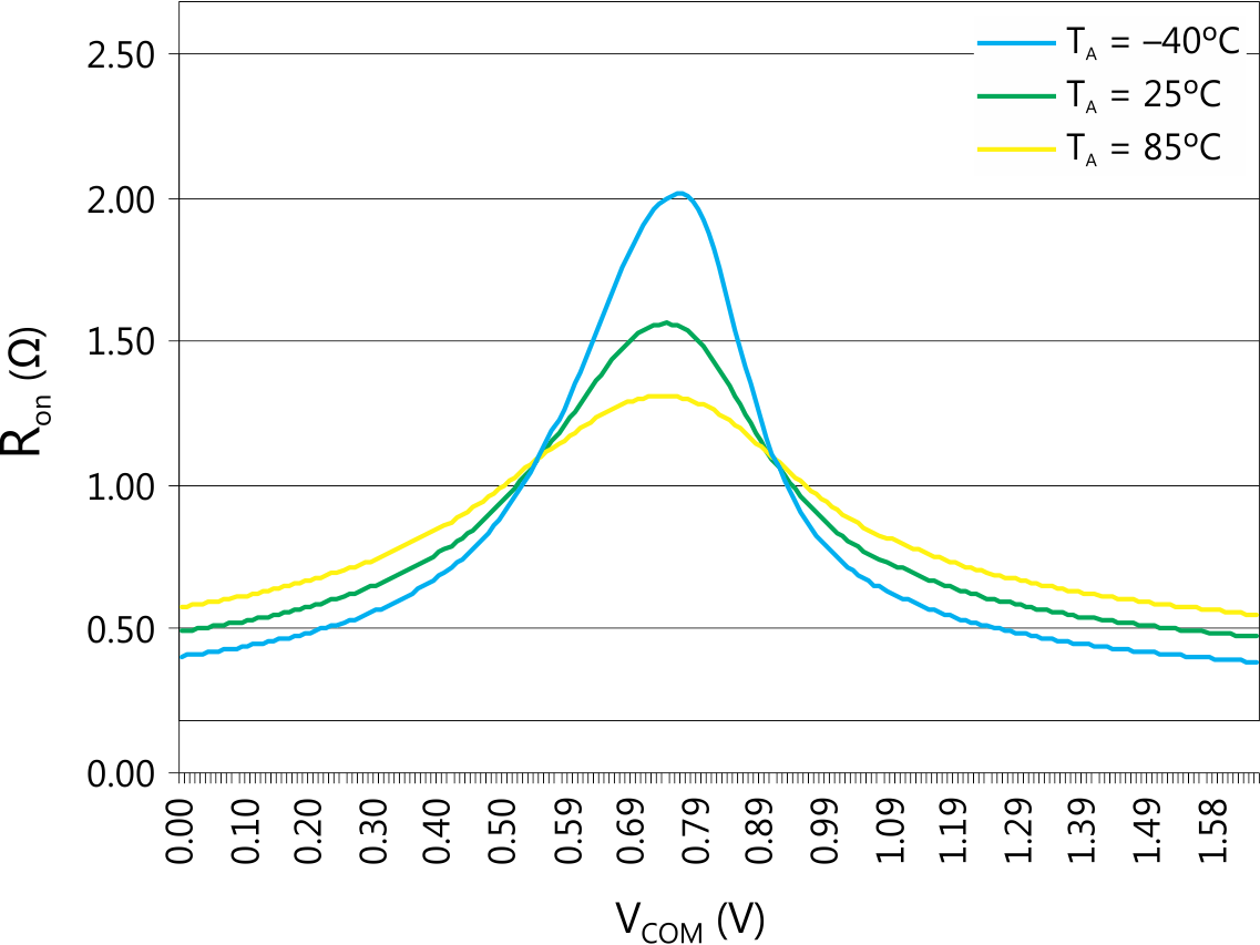 Figure 1. Ron vs VCOM (VCC = 1.65 V)
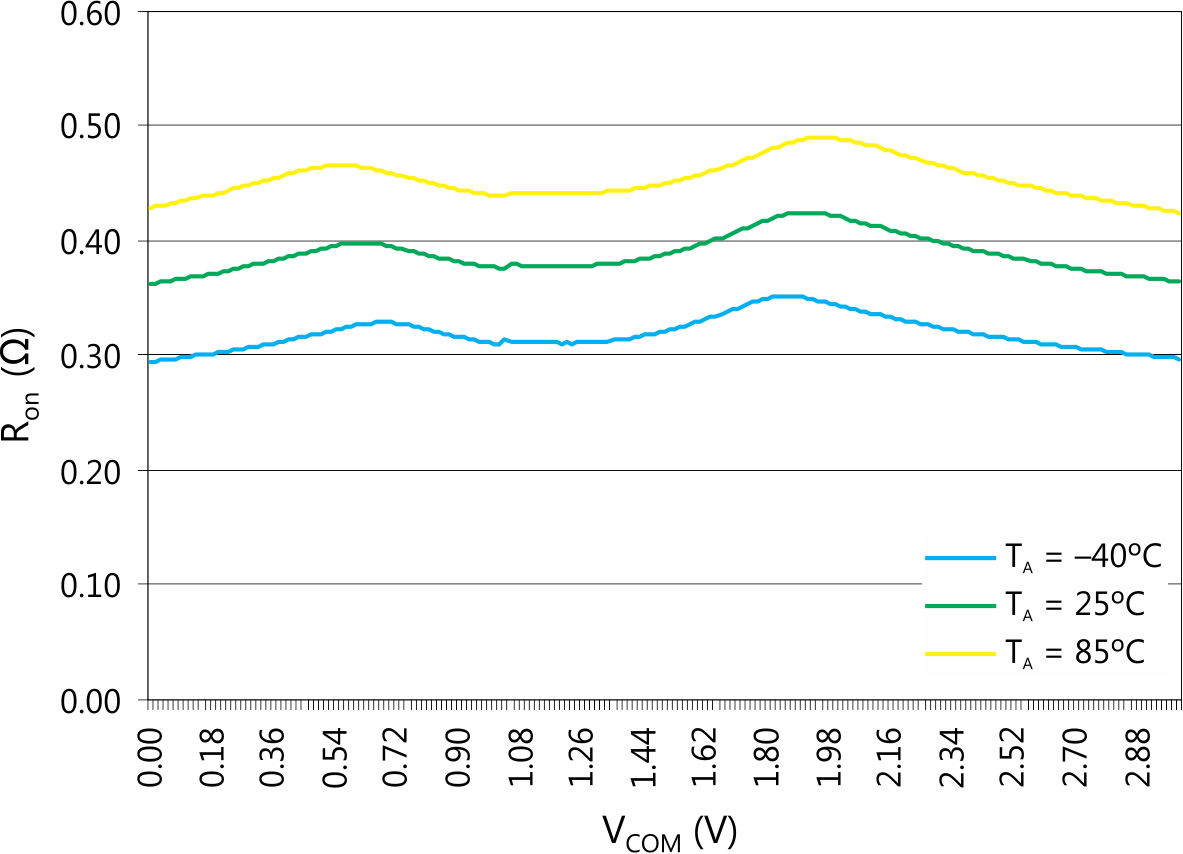 Figure 3. Ron vs VCOM (VCC = 3 V)
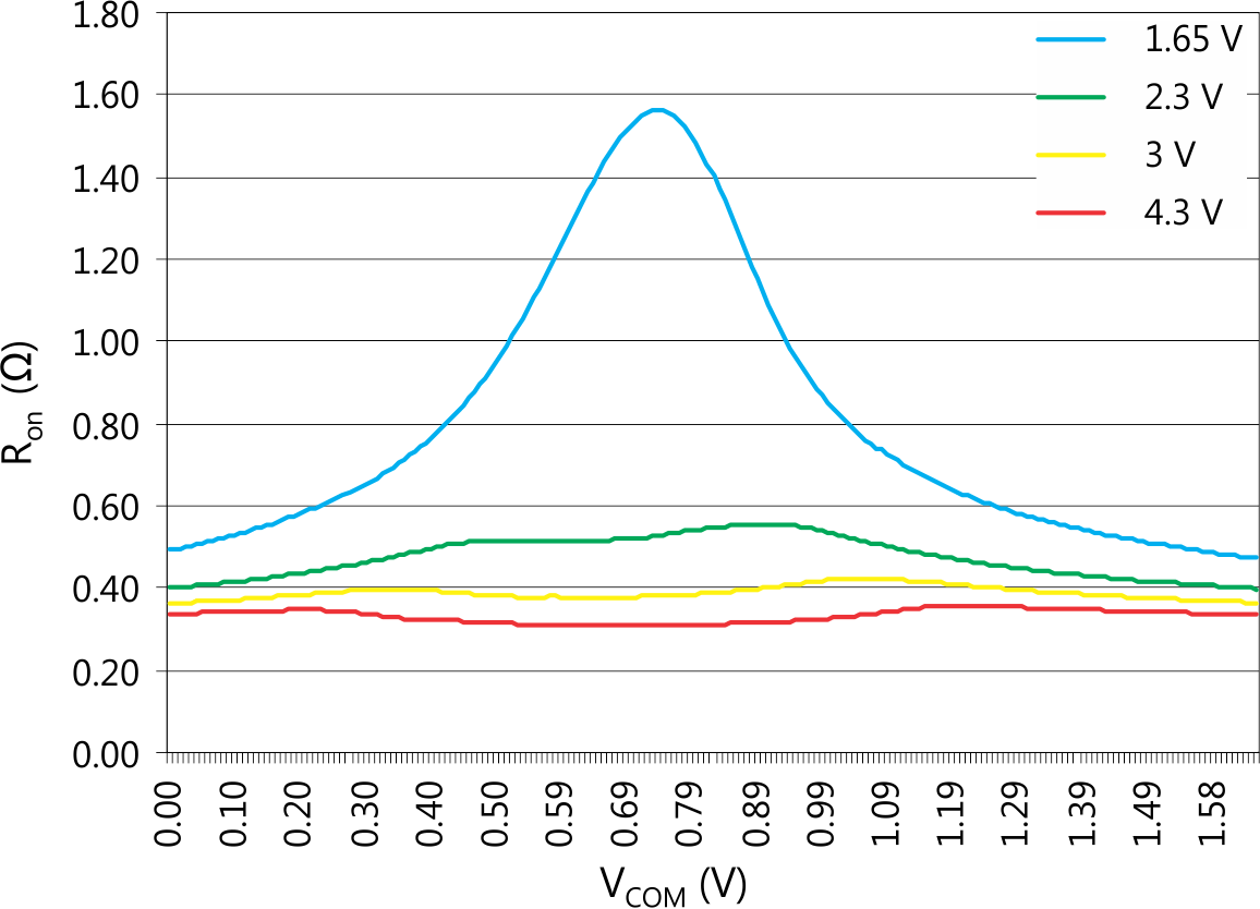 Figure 5. Ron vs VCOM (All Voltages)
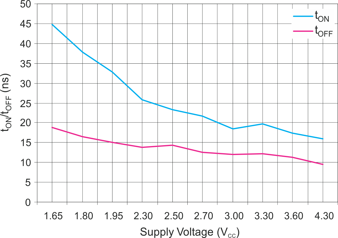 Figure 7. tON and tOFF vs Supply Voltage (TA = 25°C)
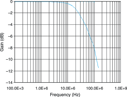 Figure 9. Bandwidth
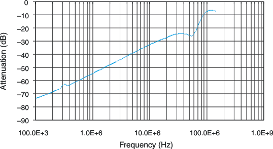 Figure 11. Crosstalk
(VCC = 2.5 V)
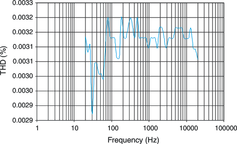
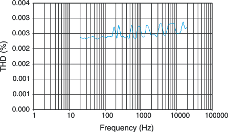 Figure 15. Total Harmonic Distortion vs Frequency (VCC = 4.3 V)
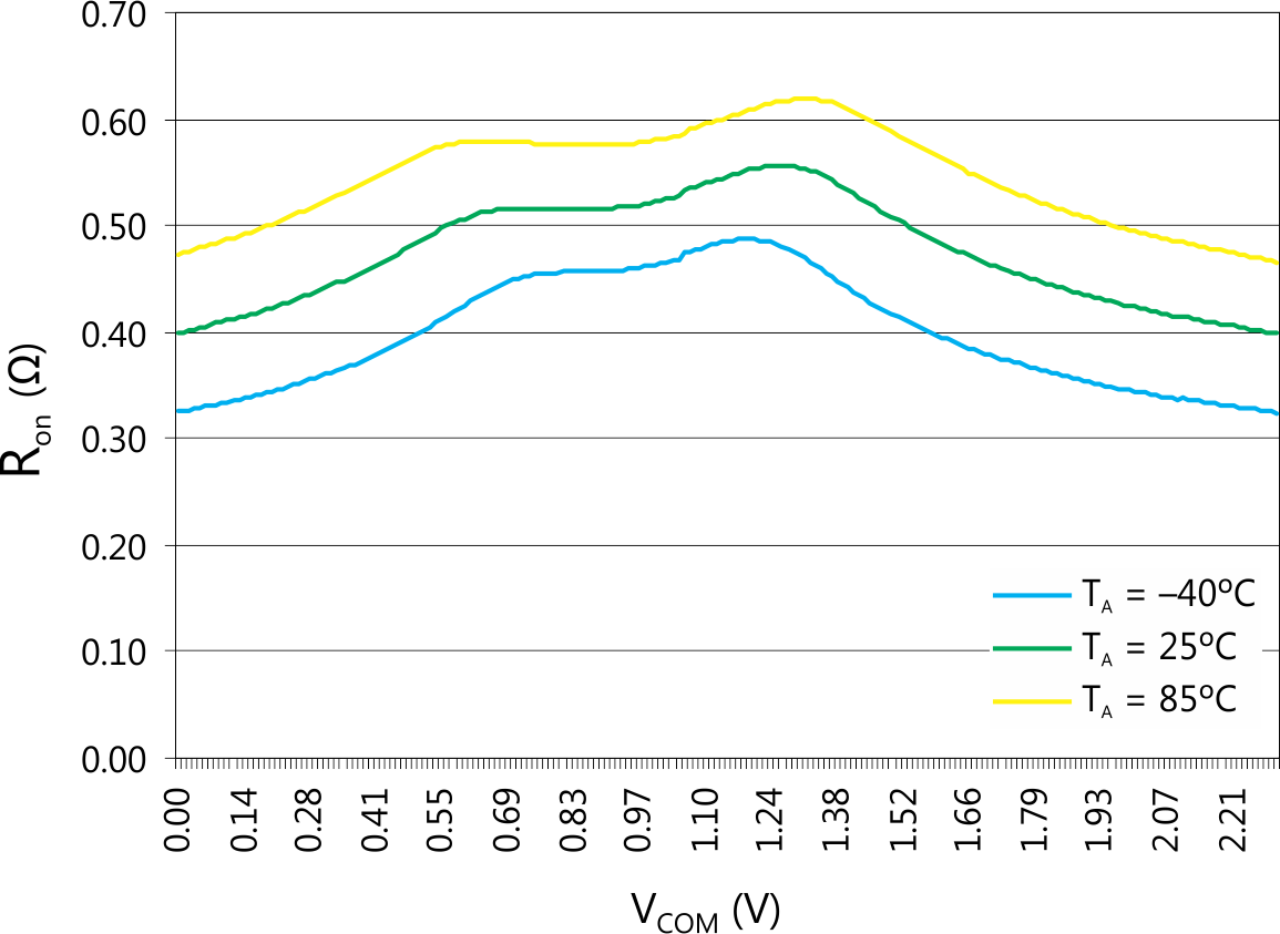 Figure 2. Ron vs VCOM (VCC = 2.3 V)
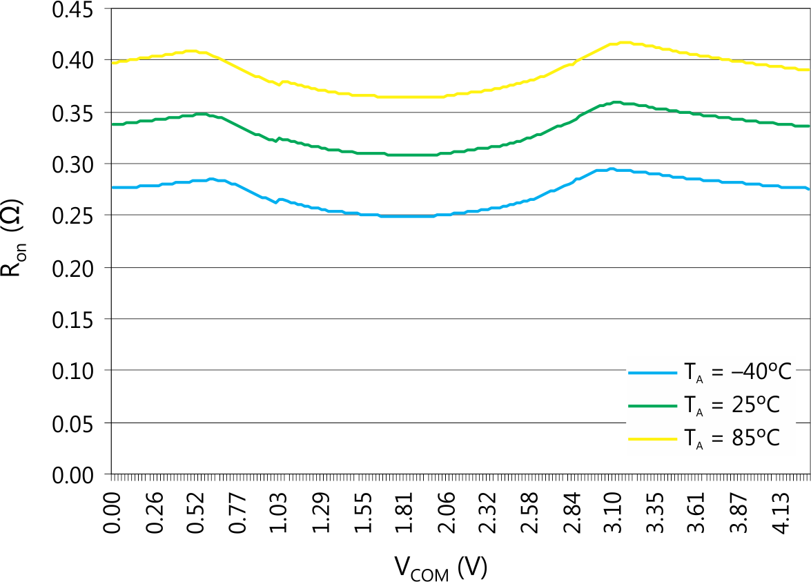 Figure 4. Ron vs VCOM (VCC = 4.3 V)
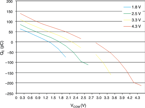 Figure 6. Charge Injection (QC) vs VCOM (TA = 25°C)
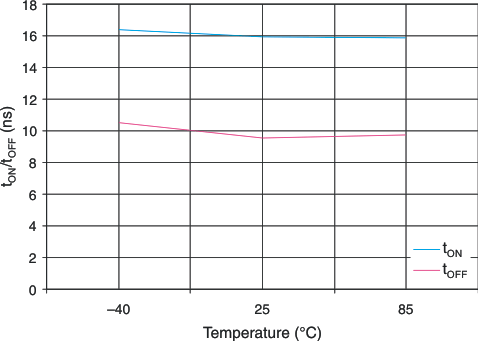 Figure 8. tON and tOFF vs Temperature (VCC = 4.3 V)
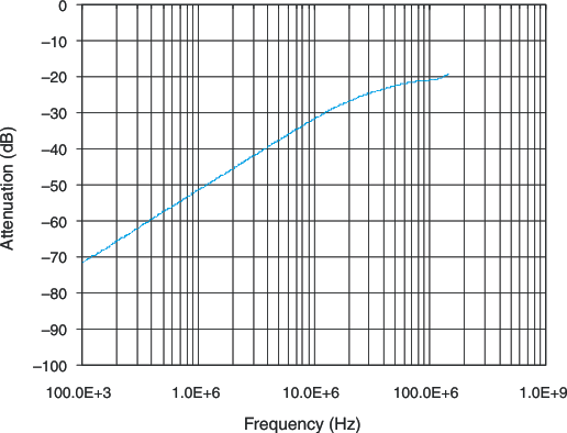 Figure 10. OFF Isolation
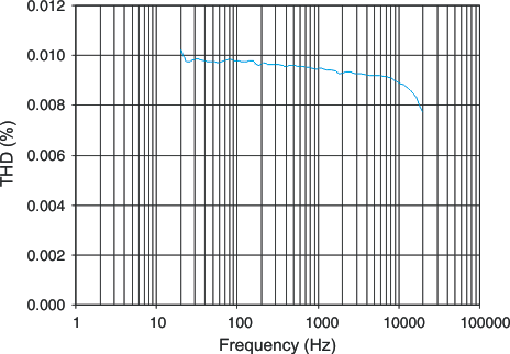
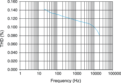 Figure 12. Total Harmonic Distortion vs Frequency
 (VCC = 1.8 V)
(VCC = 3.3 V)