ZHCS904I May 2012 – March 2017 TRF7964A
PRODUCTION DATA.
- 1器件概述
- 2修订历史记录
- 3Device Characteristics
- 4Terminal Configuration and Functions
- 5Specifications
-
6Detailed Description
- 6.1 Overview
- 6.2 System Block Diagram
- 6.3 Power Supplies
- 6.4 Receiver - Analog Section
- 6.5 Receiver - Digital Section
- 6.6 Oscillator Section
- 6.7 Transmitter - Analog Section
- 6.8 Transmitter - Digital Section
- 6.9 Transmitter - External Power Amplifier and Subcarrier Detector
- 6.10 TRF7964A IC Communication Interface
- 6.11 TRF7964A Initialization
- 6.12 Special Direct Mode for Improved MIFARE Compatibility
- 6.13
Direct Commands from MCU to Reader
- 6.13.1
Command Codes
- 6.13.1.1 Idle (0x00)
- 6.13.1.2 Software Initialization (0x03)
- 6.13.1.3 Reset FIFO (0x0F)
- 6.13.1.4 Transmission With CRC (0x11)
- 6.13.1.5 Transmission Without CRC (0x10)
- 6.13.1.6 Delayed Transmission With CRC (0x13)
- 6.13.1.7 Delayed Transmission Without CRC (0x12)
- 6.13.1.8 Transmit Next Time Slot (0x14)
- 6.13.1.9 Block Receiver (0x16)
- 6.13.1.10 Enable Receiver (0x17)
- 6.13.1.11 Test Internal RF (RSSI at RX Input With TX ON) (0x18)
- 6.13.1.12 Test External RF (RSSI at RX Input with TX OFF) (0x19)
- 6.13.1
Command Codes
- 6.14
Register Description
- 6.14.1 Register Preset
- 6.14.2 Register Overview
- 6.14.3
Detailed Register Description
- 6.14.3.1 Main Configuration Registers
- 6.14.3.2
Control Registers - Sublevel Configuration Registers
- 6.14.3.2.1 ISO/IEC 14443 TX Options Register (0x02)
- 6.14.3.2.2 ISO/IEC 14443 High-Bit-Rate and Parity Options Register (0x03)
- 6.14.3.2.3 TX Timer High Byte Control Register (0x04)
- 6.14.3.2.4 TX Timer Low Byte Control Register (0x05)
- 6.14.3.2.5 TX Pulse Length Control Register (0x06)
- 6.14.3.2.6 RX No Response Wait Time Register (0x07)
- 6.14.3.2.7 RX Wait Time Register (0x08)
- 6.14.3.2.8 Modulator and SYS_CLK Control Register (0x09)
- 6.14.3.2.9 RX Special Setting Register (0x0A)
- 6.14.3.2.10 Regulator and I/O Control Register (0x0B)
- 6.14.3.3
Status Registers
- 6.14.3.3.1 IRQ Status Register (0x0C)
- 6.14.3.3.2 Interrupt Mask Register (0x0D) and Collision Position Register (0x0E)
- 6.14.3.3.3 RSSI Levels and Oscillator Status Register (0x0F)
- 6.14.3.3.4 Special Functions Register (0x10)
- 6.14.3.3.5 Special Functions Register (0x11)
- 6.14.3.3.6 Adjustable FIFO IRQ Levels Register (0x14)
- 6.14.3.4 Test Registers
- 6.14.3.5 FIFO Control Registers
- 7Applications, Implementation, and Layout
- 8器件和文档支持
- 9机械、封装和可订购信息
7 Applications, Implementation, and Layout
NOTE
Information in the following Applications section is not part of the TI component specification, and TI does not warrant its accuracy or completeness. TI's customers are responsible for determining suitability of components for their purposes. Customers should validate and test their design implementation to confirm system functionality.
7.1 TRF7964A Reader System Using SPI With SS Mode
7.1.1 General Application Considerations
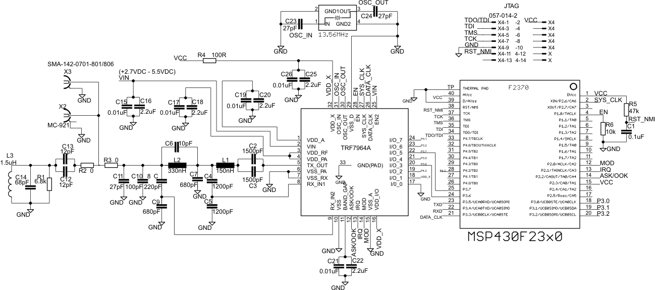
Figure 7-1 shows and application schematic optimized for all TRF7964A modes using the Serial Port Interface (SPI). Short SPI lines, proper isolation of radio frequency lines, and a proper ground area are essential to avoid interference. The recommended clock frequency on the DATA_CLK line is 2 MHz. This figure also shows matching to a 50-Ω port, which allows connecting to a properly matched 50-Ω antenna circuit or RF measurement equipment (for example, a spectrum analyzer or power meter).
7.1.2 Schematic
Figure 7-1 shows a sample application schematic for SPI with an SS mode MCU interface.
 Figure 7-1 Application Schematic – SPI With SS Mode MCU Interface
Minimum MCU requirements depend on application requirements and coding style. If only one ISO protocol or a limited command set of a protocol needs to be supported, MCU Flash and RAM requirements can be significantly reduced. Recursive inventory and anticollision commands require more RAM than single slotted operations. For example, an ISO/IEC 15693-only application that supports anticollision needs approximately 7KB of flash memory and 500 bytes of RAM. In contrast, a full NFC stack that supports peer-to-peer, card emulation, and reader/writer modes needs 65KB of flash memory and 4KB of RAM. An MCU that can run its GPIOs at 13.56 MHz is required for direct mode 0 operations.
7.2 Layout Considerations
Keep all decoupling capacitors as close to the IC as possible, with the high-frequency decoupling capacitors (10 nF) closer than the low-frequency decoupling capacitors (2.2 µF).
Place ground vias as close as possible to the ground side of the capacitors and reader IC pins to minimize possible ground loops.
TI recommends not using any inductor sizes smaller than 0603, as the output power can be compromised. If smaller inductors are necessary, output performance must be confirmed in the final application.
Pay close attention to the required load capacitance of the crystal, and adjust the two external shunt capacitors accordingly. Follow the recommendations of the crystal manufacturer for those values.
There should be a common ground plane for the digital and analog sections. The multiple ground sections or islands should have vias that tie the different sections of the planes together.
Ensure that the exposed thermal pad at the center of the reader IC is properly laid out. It should be tied to ground to help dissipate any heat from the package.
All trace line lengths should be made as short as possible, particularly the RF output path, crystal connections, and control lines from the reader to the microprocessor. Proper placement of the TRF7964A, microprocessor, crystal, and RF connection or connector help facilitate this.
Avoid crossing of digital lines under RF signal lines. Also, avoid crossing of digital lines with other digital lines when possible. If the crossings are unavoidable, 90° crossings should be used to minimize coupling of the lines.
Depending on the production test plan, consider possible implementations of test pads or test vias for use during testing. The necessary pads or vias should be placed in accordance with the proposed test plan to enable easy access to those test points.
If the system implementation is complex (for example, if the RFID reader module is a subsystem of a greater system with other modules (microprocessors and clocks), special considerations should be taken to ensure that there is no noise coupling into the supply lines. If needed, special filtering or regulator considerations should be used to minimize or eliminate noise in these systems.
For more information/details on layout considerations, see the TRF796x HF-RFID Reader Layout Design Guide.
7.3 Impedance Matching TX_Out (Pin 5) to 50 Ω
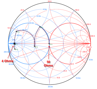
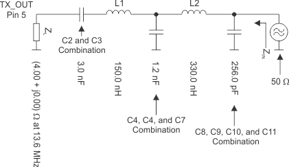
The output impedance of the TRF7964A when operated at full power out setting is nominally 4 + j0 (4 Ω real). This impedance must be matched to a resonant circuit and TI recommends matching circuit from 4 Ω to 50 Ω, as commercially available test equipment (for example, spectrum analyzers, power meters, and network analyzers) are 50-Ω systems. Figure 7-2 shows an impedance-matching reference circuit. Figure 7-3 shows a Smith chart simulation based on this circuit. This section explains how the values were calculated.
Starting with the 4-Ω source, the process of going from 4 Ω to 50 Ω can be represented on a Smith Chart simulator (available from http://www.fritz.dellsperger.net/). The elements are combined where appropriate (see Figure 7-2).
 Figure 7-3 Smith Chart Simulation
Resulting power out can be measured with a power meter or spectrum analyzer with power meter function or other equipment capable of making a "hot" measurement. Observe maximum power input levels on test equipment and use attenuators whenever available to avoid damage to equipment. Expected output power levels under various operating conditions are shown in Table 6-20.
7.4 Reader Antenna Design Guidelines
For HF antenna design considerations using the TRF7964A, see these documents:
