SLWS213A January 2010 – November 2015 TRF370417
PRODUCTION DATA.
- 1 Features
- 2 Applications
- 3 Description
- 4 Revision History
- 5 Pin Configuration and Functions
- 6 Specifications
- 7 Detailed Description
- 8 Application and Implementation
- 9 Power Supply Recommendations
- 10Layout
- 11Device and Documentation Support
- 12Mechanical, Packaging, and Orderable Information
封装选项
机械数据 (封装 | 引脚)
- RGE|24
散热焊盘机械数据 (封装 | 引脚)
- RGE|24
订购信息
10 Layout
10.1 Layout Guidelines
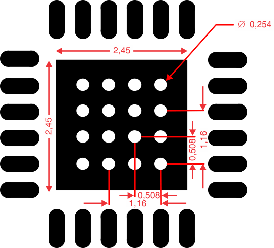
The TRF370417 device is fitted with a ground slug on the back of the package that must be soldered to the printed circuit board (PCB) ground with adequate ground vias to ensure a good thermal and electrical connection. The recommended via pattern and ground pad dimensions are shown in Figure 76. The recommended via diameter is 10 mils (0.10 in or 0.25 mm). The ground pins of the device can be directly tied to the ground slug pad for a low-inductance path to ground. Additional ground vias may be added if space allows. Decoupling capacitors at each of the supply pins are strongly recommended. The value of these capacitors should be chosen to provide a low-impedance RF path to ground at the frequency of operation. Typically, the value of these capacitors is approximately 10 pF or lower. The device exhibits symmetry with respect to the quadrature input paths. TI recommends that the PCB layout maintain this symmetry to ensure that the quadrature balance of the device is not impaired. The I/Q input traces should be routed as differential pairs and the respective lengths all kept equal to each other. On the RF traces, maintain proper trace widths to keep the characteristic impedance of the RF traces at a nominal 50 Ω.
10.2 Layout Example
Figure 44 shows the top view of the TRF3704 EVM board.
 Figure 44. PCB Via Ground Layout Guide