SLWS213A January 2010 – November 2015 TRF370417
PRODUCTION DATA.
- 1 Features
- 2 Applications
- 3 Description
- 4 Revision History
- 5 Pin Configuration and Functions
- 6 Specifications
- 7 Detailed Description
- 8 Application and Implementation
- 9 Power Supply Recommendations
- 10Layout
- 11Device and Documentation Support
- 12Mechanical, Packaging, and Orderable Information
封装选项
机械数据 (封装 | 引脚)
- RGE|24
散热焊盘机械数据 (封装 | 引脚)
- RGE|24
订购信息
7 Detailed Description
7.1 Overview
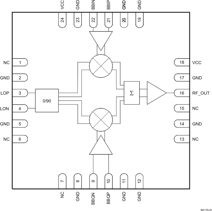
TRF370417 is a low-noise direct quadrature modulator with high linearity, capable of converting complex modulated signals from baseband or IF directly to RF. With high-performance and superior-linearity, the TRF370417 is an ideal device to up-convert to RF frequencies from 50-MHz through 6-GHz. The baseband inputs can support an input bandwidth up to 1-GHz. The modulator is implemented as a double-balanced mixer. The RF output block contains a differential to single-ended converter to drive a 50-ohm load without the need for external matching components. The baseband input common-mode voltage is set at 1.7-V for optimum linearity performance.
7.2 Functional Block Diagram

NOTE:
NC = No connection7.3 Feature Description
TRF370417 supports an I/Q baseband input bandwidth of 1-GHz. With this bandwidth capability the input signal can be centered at a high IF frequency to provide frequency separation from unwanted carrier feed-through or sideband image. Utilizing the full baseband bandwidth yields an RF output bandwidth up to 2-GHz.
7.4 Device Functional Modes
7.4.1 Baseband Common-Mode Voltage
TRF370417 input baseband pins operate around a common-mode voltage of 1.7-V. Variation around this common-mode is possible but best linearity performance is generally achieved when kept at nominal voltage.
7.4.2 LO Drive Level
The LO drive level is nominally specified at 4-dBm. The device can accept a large range of LO drive level. A higher drive level generally provides better output noise performance and some linearity improvement. There is some trade-off between carrier feed-through and sideband suppression performance that is dependent on frequency and drive level. The LO drive level of 4-dB is deemed a good balance between those two parameters across frequency.