ZHCSLX4A October 2020 – December 2020 TPSM41615
PRODUCTION DATA
- 1 特性
- 2 应用
- 3 说明
- 4 Revision History
- 5 Pin Configuration and Functions
- 6 Specifications
-
7 Detailed Description
- 7.1 Overview
- 7.2 Functional Block Diagram
- 7.3
Feature Description
- 7.3.1 Setting the Output Voltage
- 7.3.2 RS+/RS- Remote Sense Function
- 7.3.3 Ramp Select (RAMP and RAMP_SEL)
- 7.3.4 Switching Frequency (RT)
- 7.3.5 Synchronization (SYNC)
- 7.3.6 Stand-alone/Stackable Operation
- 7.3.7 Improved Transient Performance versus Fixed Frequency (Stand-alone Operation Only)
- 7.3.8 Output On/Off Enable (EN)
- 7.3.9 Power Good (PGOOD)
- 7.3.10 Soft-Start Operation
- 7.3.11 Input Capacitor Selection
- 7.3.12 Output Capacitor Selection
- 7.3.13 Current Limit (ILIM)
- 7.3.14 Safe Start-up into Pre-Biased Outputs
- 7.3.15 Overcurrent Protection
- 7.3.16 Output Overvoltage and Undervoltage Protection
- 7.3.17 Overtemperature Protection
- 7.4 Device Functional Modes
- 8 Application and Implementation
- 9 Power Supply Recommendations
- 10Layout
- 11Device and Documentation Support
- 12Mechanical, Packaging, and Orderable Information
7.3.1 Setting the Output Voltage
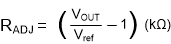
The output voltage adjustment range of the TPSM41615 is 0.6 V to 7.1 V. Setting the output voltage requires first setting the internal reference voltage (VREF). The internal reference voltage can be set from 0.6 V to 1.1 V using a resistor (RVSEL) connected from VSEL (pin 28) to AGND (pin 19). Table 7-1 lists reference voltage selections and their corresponding setting resistors. If the required output voltage is the same as the reference voltage, connect the RS+ pin (pin 35) directly to VOUT to set the output voltage as shown in Figure 7-1. Output voltages greater than the reference voltage require an external voltage setting resistor (RADJ) between the RS+ pin and VOUT to set the output voltage as shown in Figure 7-2. The value for RADJ can be calculated using Equation 1 or simply selected from the recommended values given in Table 7-2. Additionally, Table 7-3 includes the recommended switching frequency (FSW), the recommended Ramp resistor (RRAMP), and the minimum output capacitance for several output voltage ranges.
When setting the output voltage, selecting the highest reference voltage will result in the most accurate output voltage set point. The output voltage will be regulated at the connection point of RS+ or RADJ to VOUT. Making the connection near the load improves regulation at the load.
| VREF (V) | 0.6 | 0.7 | 0.75 | 0.8 | 0.85 | 0.9 | 0.95 | 1.0 | 1.05 | 1.1 |
| RVSEL Value (kΩ)(1) | 0 | 8.66 | 15.4 | 23.7 | 34.8 | 51.1 | 78.7 | open | 121 | 187 |
| VOUT (V) | 0.6 - 1.1 | 1.2 | 1.5 | 1.8 | 2.5 | 3.3 | 5.0 | 6.0 | 7.0 |
| VREF (V)(1) | 0.6 - 1.1 | 1.1 | 1.1 | 1.1 | 1.1 | 1.1 | 1.1 | 1.1 | 1.1 |
| RADJ Value (Ω)(1) | short | 90.9 | 365 | 634 | 1270 | 2000 | 3570 | 4420 | 5360 |
") Figure 7-1 Setting the Output Voltage
Figure 7-1 Setting the Output Voltage(VOUT = VREF)
") Figure 7-2 Setting the Output Voltage
Figure 7-2 Setting the Output Voltage(VOUT > VREF)
| PVIN = 5 V | ||||||
|---|---|---|---|---|---|---|
| VOUT RANGE (V) | RECOMMENDED FSW (kHz)(1) | ALLOWABLE FSW RANGE (KHZ) | RRAMP (kΩ) | MINIMUM REQUIRED COUT (µF)(4) | ||
| MIN | MAX | MINIMUM CERAMIC(3) | ADDITIONAL REQUIRED CAPACITANCE(5) | |||
| 0.6 | < 0.8 | 400 | 300 - < 450 | 78.7 | 294(2) | 610 |
| 500 | 450 - < 550 | 187 | 490 | |||
| 600 | 550 - < 700 | 187 | 300 | |||
| 700 | 700 - 1000 | 78.7 | 280 | |||
| 0.8 | < 1.0 | 400 | 300 - < 450 | 78.7 | 289(2) | 600 |
| 500 | 450 - < 850 | 78.7 | 420 | |||
| 900 | 850 - 1000 | 78.7 | 240 | |||
| 1.0 | < 1.2 | 500 | 400 - 1000 | 187 | 284(2) | 190 |
| 1.2 | < 1.5 | 500 | 400 - 1000 | 187 | 277(2) | 100 |
| 1.5 | < 1.8 | 500 | 400 - 1000 | 187 | 266(2) | 90 |
| 1.8 | < 2.5 | 500 | 400 - 1000 | 187 | 254(2) | 85 |
| 2.5 | 3.3 | 500 | 400 - 1000 | 78.7 | 224(2) | 65 |
| PVIN = 12 V | ||||||
| VOUT RANGE (V) | RECOMMENDED FSW (kHz)(1) | ALLOWABLE FSW RANGE (kHz) | RRAMP (kΩ) | MINIMUM REQUIRED COUT (µF)(4) | ||
| MIN | MAX | MINIMUM CERAMIC(3) | ADDITIONAL REQUIRED CAPACITANCE(5) | |||
| 0.6 | < 1.0 | 400 | 350 - < 450 | 78.7 | 294(2) | 760 |
| 500 | 450 - < 550 | 78.7 | 430 | |||
| 600 | 550 - 750 | 78.7 | 250 | |||
| 1.0 | < 1.2 | 400 | 350 - < 500 | 78.7 | 284(2) | 760 |
| 550 | 500 - < 600 | 78.7 | 430 | |||
| 600 | 600 - 1000 | 78.7 | 250 | |||
| 1.2 | < 1.8 | 400 | 350 - < 500 | 78.7 | 277(2) | 760 |
| 500 | 500 - < 600 | 121 | 185 | |||
| 600 | 600 - 1000 | 121 | 100 | |||
| 1.8 | < 2.5 | 400 | 350 - < 500 | 78.7 | 254(2) | 600 |
| 500 | 500 - < 600 | 187 | 430 | |||
| 600 | 600 - < 850 | 187 | 250 | |||
| 700 | 850 - 1000 | 78.7 | 90 | |||
| 2.5 | < 3.3 | 500 | 450 - < 650 | 78.7 | 224(2) | 450 |
| 700 | 650 - < 950 | 187 | 80 | |||
| 1000 | 950 - 1000 | 121 | 80 | |||
| 3.3 | < 5.0 | 600 | 550 - 1000 | 187 | 191(2) | 65 |
| 5.0 | 7.1 | 700 | 600 - 1000 | 187 | 134(2) | 0 |