ZHCSAO9A December 2012 – September 2015 TPS92690
PRODUCTION DATA.
- 1 特性
- 2 应用
- 3 说明
- 4 修订历史记录
- 5 Pin Configuration and Functions
- 6 Specifications
-
7 Detailed Description
- 7.1 Overview
- 7.2 Functional Block Diagram
- 7.3
Feature Description
- 7.3.1 Current Regulators
- 7.3.2 Peak Current Mode Control
- 7.3.3 Switching Frequency and Synchronization
- 7.3.4 Current Sense and Current Limit
- 7.3.5 Average LED Current
- 7.3.6 Precision Reference (VREF)
- 7.3.7 Low-Level Analog Dimming
- 7.3.8 Soft-Start and Shutdown
- 7.3.9 VCC Regulator and Start-Up
- 7.3.10 Overvoltage Protection (OVP)
- 7.3.11 Input Undervoltage Lockout (UVLO)
- 7.3.12 PWM Dimming
- 7.3.13 Control Loop Compensation
- 7.3.14 Thermal Shutdown
- 7.4 Device Functional Modes
-
8 Application and Implementation
- 8.1 Application Information
- 8.2
Typical Applications
- 8.2.1
Basic Topology Schematics
- 8.2.1.1 Design Requirements
- 8.2.1.2
Detailed Design Procedure
- 8.2.1.2.1 Operating Point
- 8.2.1.2.2 Switching Frequency
- 8.2.1.2.3 Average LED Current
- 8.2.1.2.4 Inductor Ripple Current
- 8.2.1.2.5 Output Capacitance
- 8.2.1.2.6 Peak Current Limit
- 8.2.1.2.7 Loop Compensation
- 8.2.1.2.8 Input Capacitance
- 8.2.1.2.9 NFET
- 8.2.1.2.10 Diode
- 8.2.1.2.11 Input UVLO
- 8.2.1.2.12 Output OVLO
- 8.2.1.3 Application Curve
- 8.2.2
Simplified Application
- 8.2.2.1 Design Requirements
- 8.2.2.2
Detailed Design Procedure
- 8.2.2.2.1 Operating Point
- 8.2.2.2.2 Switching Frequency
- 8.2.2.2.3 Average LED Current
- 8.2.2.2.4 Inductor Ripple Current
- 8.2.2.2.5 LED Ripple Current
- 8.2.2.2.6 Peak Current Limit
- 8.2.2.2.7 Loop Compensation
- 8.2.2.2.8 Input Capacitance
- 8.2.2.2.9 NFET
- 8.2.2.2.10 Diode
- 8.2.2.2.11 Output OVLO
- 8.2.2.2.12 Input UVLO
- 8.2.2.2.13 Soft-Start
- 8.2.2.2.14 PWM Dimming Method
- 8.2.2.2.15 Analog Dimming Method
- 8.2.1
Basic Topology Schematics
- 9 Power Supply Recommendations
- 10Layout
- 11器件和文档支持
- 12机械、封装和可订购信息
8 Application and Implementation
NOTE
Information in the following applications sections is not included in the TI component specification, and TI does not warrant its accuracy or completeness. TI customers are responsible for determining suitability of components for their purposes. Customers should validate and test their design implementation to confirm system functionality.
8.1 Application Information
8.1.1 Inductor
The inductor (L1) is the main energy storage device in a switching regulator. Depending on the topology, energy is stored in the inductor and transferred to the load in different ways (as an example, boost operation is detailed in the Current Regulators section). The size of the inductor, the voltage across it, and the length of the switching subinterval (tON or tOFF) determines the inductor current ripple (ΔiL-PP). In the design process, L1 is chosen to provide a desired ΔiL-PP. For a Cuk regulator the second inductor (L2) has a direct connection to the load, which is good for a current regulator. This requires little to no output capacitance therefore ΔiL-PP is basically equal to the LED ripple current ΔiLED-PP since the inductor ripple in L2 is equal to that in L1. However, for boost and other buck-boost regulators, there is always an output capacitor which reduces ΔiLED-PP, therefore the inductor ripple can be larger than in the Cuk regulator case where output capacitance is minimal or completely absent.
In general, ΔiLED-PP is recommended by manufacturers to be less than 40% of the average LED current (ILED). Therefore, for the Cuk regulator with no output capacitance, ΔiLED-PP should also be less than 40% of ILED unless a large output capacitor is used. For the boost and other buck-boost topologies, ΔiL-PP can be much higher depending on the output capacitance value. However, ΔiL-PP is suggested to be less than 100% of the average inductor current (iL) to limit the RMS inductor current. ΔiL-PP is defined as:

Be sure to observe the minimum inductor value from the Control Loop Compensation section. L1 is also suggested to have an RMS current rating at least 25% higher than the calculated minimum allowable RMS inductor current (IL-RMS).
8.1.2 LED Dynamic Resistance
When the load is a string of LEDs, the output load resistance is the LED string dynamic resistance plus RCS. LEDs are PN junction diodes, and their dynamic resistance shifts as their forward current changes. Dividing the forward voltage of a single LED (VLED) by the forward current (ILED) can lead to an incorrect calculation of the dynamic resistance of a single LED (rLED). The result can be 5 to 10 times higher than the true rLED value.
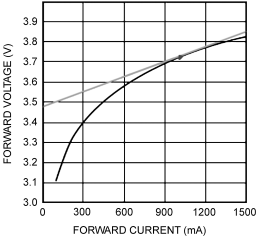 Figure 18. Dynamic Resistance
Obtaining rLED is accomplished by referring to the manufacturer LED I-V characteristic. It can be calculated as the slope at the nominal operating point as shown in Figure 18. For any application with more than 2 series LEDs, RCS can be neglected allowing rD to be approximated as the number of LEDs multiplied by rLED.
8.1.3 Output Capacitor
For boost, SEPIC, and flyback regulators, the output capacitor (CO) provides energy to the load when the recirculating diode (D1) is reverse biased during the first switching subinterval. An output capacitor in a Cuk topology simply reduces the LED current ripple (ΔiLED-PP) below the inductor current ripple (ΔiL-PP). In all cases, CO is sized to provide a desired ΔiLED-PP. As mentioned in Inductor, ΔiLED-PP is recommended by manufacturers to be <40% of the average LED current (ILED).
CO should be carefully chosen to account for derating due to temperature and operating voltage. It must also have the necessary RMS current rating. Ceramic capacitors are the best choice due to their high ripple current rating, long lifetime, and good temperature performance. An X7R dielectric rating is suggested.
8.1.4 Input Capacitor
The input capacitor (CIN) only needs to provide the ripple current due to the direct connection to the inductor. CIN is selected given the maximum input voltage ripple (ΔVIN-PP) which can be tolerated. ΔVIN-PP is suggested to be less than 10% of the input voltage (VIN). An input capacitance at least 100% greater than the calculated CIN value is recommended to account for derating due to temperature and operating voltage. When PWM dimming, even more capacitance can be helpful to minimize the large current draw from the input voltage source during the rising transition of the LED current waveform.
The chosen input capacitors must also have the necessary RMS current rating. Ceramic capacitors are again the best choice due to their high ripple current rating, long lifetime, and good temperature performance. An X7R dielectric rating is suggested.
For most applications, it is recommended to bypass the VIN pin with an 0.1-µF ceramic capacitor placed as close as possible to the pin. In situations where the bulk input capacitance may be far from the TPS92690 device, a 10-Ω series resistor can be placed between the bulk input capacitance and the bypass capacitor, creating a 150-kHz filter to eliminate undesired high frequency noise.
8.1.5 MOSFET Selection
The TPS92690 device requires an external N-channel FET (Q1) as the main power MOSFET for the switching regulator. Q1 is recommended to have a voltage rating at least 15% higher than the maximum transistor voltage to ensure safe operation during the ringing of the switch node. In practice, all switching regulators have some ringing at the switch node due to the diode parasitic capacitance and the lead inductance. The current rating is recommended to be at least 10% higher than the average transistor current. The power rating is then verified by calculating the power loss given the average transistor current and the N-channel FET on-resistance (RDS(on)).
In general, the N-channel FET should be chosen to minimize total gate charge (Qg) when ƒSW is high and minimize RDS(on) otherwise. This minimizes the dominant power losses in the system. Frequently, higher current N-channel FETs in larger packages are chosen for better thermal performance.
8.1.6 Recirculating Diode
A recirculating diode (D1) is required to carry the inductor current during tOFF. The most efficient choice for D1 is a Schottky diode due to low forward voltage drop and near-zero reverse recovery time. Similar to Q1, D1 is recommended to have a voltage rating at least 15% higher than the maximum transistor voltage to ensure safe operation during the ringing of the switch node and a current rating at least 10% higher than the average diode current. The power rating is verified by calculating the power loss through the diode. This is accomplished by checking the typical diode forward voltage from the I-V curve on the product datasheet and multiplying by the average diode current. In general, higher current diodes have a lower forward voltage and come in better performing packages minimizing both power losses and temperature rise.
8.2 Typical Applications
8.2.1 Basic Topology Schematics
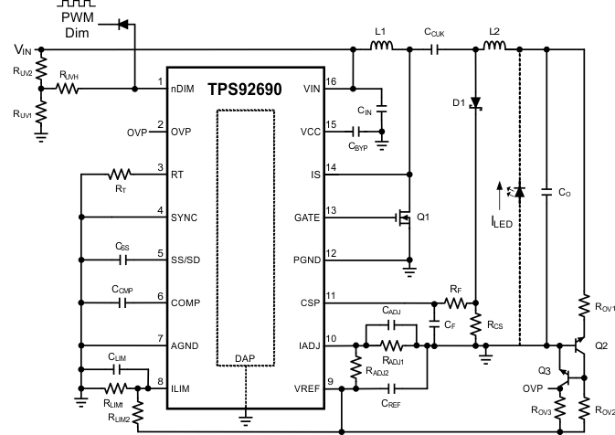 Figure 19. CUK Topology (Buck-Boost)
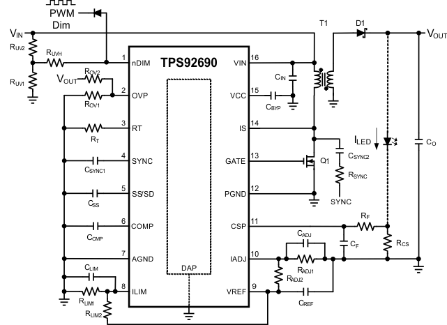 Figure 20. Quasi-Resonant Flyback Topology
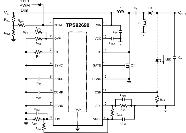 Figure 21. SEPIC Topology (Buck-Boost)
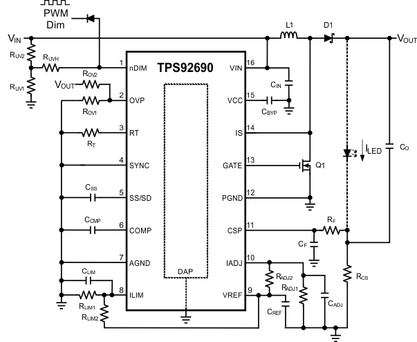 Figure 22. Boost Topology With PWM Dimming
8.2.1.1 Design Requirements
N = 10
VLED = 3.5 V
rLED = 500 mΩ
VIN = 12 V
VIN-MIN = 8 V
VIN-MAX = 19 V
fSW = 420 kHz
VCS = 50 mV
ILED = 500 mA
ΔiL-PP < 650 mA
ΔiLED-PP < 50 mA
ΔvIN-PP = 50 mV
VLIM = 100 mV
ILIM = 5 A
VTURN-ON = 7.8 V
VHYS = 2 V
VTURN-OFF = 40 V
VHYSO = 5 V
8.2.1.2 Detailed Design Procedure
8.2.1.2.1 Operating Point
Solve for VO and rD:


Solve for D, DMAX, and DMIN:


8.2.1.2.2 Switching Frequency
Solve for RT:

A close standard resistor is 105 kΩ resulting in fSW = 402 kHz. Choose RT = 105 kΩ.
8.2.1.2.3 Average LED Current
Solve for RCS using our desired 50-mV sense voltage:

Solve for VIADJ:

A resistor divider can be used from the reference pin (VREF) to IADJ, select RIAD2 = 100 kΩ and solve for RIAD1:

The closest standard value is to choose RADJ1 = 25.5 kΩ.
8.2.1.2.4 Inductor Ripple Current
Solve for the minimum value of L1 for stability:

The inductor value required to meet the ripple current requirements is:

The closest standard inductor is 33 µH therefore ΔiL-PP is:

Determine minimum allowable RMS current rating:

The chosen component is L1 = 33 µH.
8.2.1.2.5 Output Capacitance
Solve for CO:

Add some capacitance to account for voltage de-rating and temperature and choose CO = 4.7 µF.
Determine minimum allowable RMS current rating:

Since this is a PWM dimming application the output capacitor should be placed directly across the LED string and not connected to ground. So the CS pin should have additional filtering in the form of RF = 47 Ω and CF = 47 nF.
8.2.1.2.6 Peak Current Limit
Solve for RLIM:

The closest standard resistor is 0.02 Ω; therefore, choose RLIM = 0.02 Ω.
Assume RLIM2 = 100 kΩ and calculate RLIM1:

The closest standard value is RLIM1 = 4.22 kΩ
8.2.1.2.7 Loop Compensation
Check the frequency of the output pole:

Check the frequency of the RHP zero:

The lower of the two is the RHP zero at 1.64 kHz, so the maximum crossover frequency should be 164 Hz or less. Calculate the minimum COMP capacitor value:

To ensure stability over all conditions add some margin and choose CCMP = 47 nF.
8.2.1.2.8 Input Capacitance
Solve for the minimum CIN:

To minimize power supply interaction a 200% larger capacitance or more should be used particularly with PWM dimming, therefore the actual ΔvIN-PP is much lower. Choose CIN = 10 µF.
Determine minimum allowable RMS current rating:

8.2.1.2.9 NFET
Determine minimum Q1 voltage rating and current rating:


The RMS current rating used in conjunction with the chosen FET RDS-ON to calculate power dissipation is:

8.2.1.2.10 Diode
Determine minimum D1 voltage rating and current rating:


8.2.1.2.11 Input UVLO
Since this is a PWM dimming application RUVH will be used. Start by picking RUV2 = 10 kΩ and solve for RUV1:

The closest standard resistor is 1.89 kΩ so choose RUV1 = 1.89 kΩ.
Solve for RUVH given the hysteresis requirements:

The closest standard resistor is 14.3 kΩ so choose RUVH = 14.3 kΩ.
8.2.1.2.12 Output OVLO
Solve for ROV2:

The closest standard resistor is 249 kΩ; therefore, choose RUV2 = 249 kΩ. Solve for ROV1:

Choose the nearest standard resistor value of ROV1 = 8.06 kΩ.
8.2.1.3 Application Curve
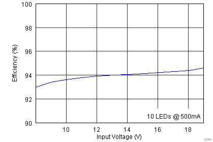 Figure 23. Efficiency vs Input Voltage
8.2.2 Simplified Application
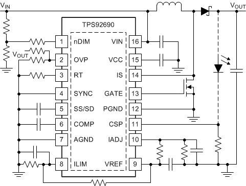 Figure 24. Simplified Application Schematic
8.2.2.1 Design Requirements
Number of series LEDs: N
Single LED forward voltage: VLED
Single LED dynamic resistance: rLED
Nominal input voltage: VIN
Input voltage range: VIN-MAX, VIN-MIN
Switching frequency: fSW
Current sense voltage: VCS
Average LED current: ILED
Inductor current ripple: ΔiL-PP
LED current ripple: ΔiLED-PP
Peak current limit: ILIM
Input voltage ripple: ΔvIN-PP
Output OVLO characteristics: VTURN-OFF, VHYSO
Input UVLO characteristics: VTURN-ON, VHYS
Total start-up time: tTSU
8.2.2.2 Detailed Design Procedure
8.2.2.2.1 Operating Point
Given the number of series LEDs (N), the forward voltage (VLED) and dynamic resistance (rLED) for a single LED, solve for the nominal output voltage (VO) and the nominal LED string dynamic resistance (rD):


Solve for the ideal nominal duty cycle (D):
Boost

Buck-Boost

Using the same equations, find the minimum duty cycle (DMIN) using maximum input voltage (VIN-MAX) and the maximum duty cycle (DMAX) using the minimum input voltage (VIN-MIN). Also, remember that D' = 1 - D.
8.2.2.2.2 Switching Frequency
Set the switching frequency (fSW) by solving for RT:

8.2.2.2.3 Average LED Current
For all topologies, set the average LED current (ILED) knowing the desired current sense voltage (VCS) and solving for RCS:


If the calculated RCS is too far from a desired standard value, then VCS will have to be adjusted to obtain a standard value.
Setup the IADJ voltage by assuming RADJ2 = 100 kΩ and solving for RADJ1:

If the calculated RADJ1 is too far from a desired standard value, then RADJ2 can be adjusted to obtain a standard value.
8.2.2.2.4 Inductor Ripple Current
Find the minimum inductor value and calculate the nominal inductor ripple current (ΔiL-PP) by solving for the appropriate inductor (L1):
8.2.2.2.4.1 Minimum Inductor Value

8.2.2.2.4.2 Inductor Ripple Current

If the inductor ripple current is too high given the chosen value increase L1 to get the required inductor current ripple. For buck-boost applications replace VO with VIN + VO when solving for L1.
The minimum allowable inductor RMS current rating (IL-RMS) can be calculated as:
8.2.2.2.4.3 RMS Inductor Current

8.2.2.2.5 LED Ripple Current
Set the nominal LED ripple current (ΔiLED-PP), by solving for the output capacitance (CO):
8.2.2.2.5.1 Output Capacitor

To set the worst case LED ripple current, use DMAX when solving for CO.
The minimum allowable RMS output capacitor current rating (ICO-RMS) can be approximated:
8.2.2.2.5.2 Output Capacitor RMS Current

8.2.2.2.6 Peak Current Limit
Set the peak current limit (ILIM) by setting the ILIM pin voltage and solving for the transistor path sense resistor (RLIM):


8.2.2.2.7 Loop Compensation
Using a simple first order peak current mode control model, neglecting any output capacitor ESR dynamics, the necessary loop compensation can be determined.
A maximum bandwidth (fC) of 10 kHz is recommended and the COMP pin capacitor can be calculated using:
8.2.2.2.7.1 Compensation Capacitor

Check the location of the right-half plane zero and the output pole and make sure the crossover frequency is at least a decade below the lowest of the two using the following equations:
8.2.2.2.7.2 RHP Zero

8.2.2.2.7.3 Output Capacitor Pole

If the input voltage range is wide use the maximum duty cycle (DMAX) corresponding to the minimum input voltage to calculate the RHP zero. In general smaller CCMP values will provide greater bandwidth but the bandwidth may be limited by the location of the RHP zero or output pole. For PWM dimming applications the largest capacitor value that will fit the applications requirements is suggested.
8.2.2.2.8 Input Capacitance
Set the nominal input voltage ripple (ΔvIN-PP) by solving for the required capacitance (CIN):
Boost

Buck-Boost

Use DMAX to set the worst case input voltage ripple.
The minimum allowable RMS input current rating (ICIN-RMS) can be approximated:
Boost

Buck-Boost

8.2.2.2.9 NFET
The NFET voltage rating should be at least 15% higher than the maximum NFET drain-to-source voltage (VT-MAX):
Boost

Buck-Bosst

The current rating should be at least 10% higher than the maximum average NFET current (IT-MAX):
8.2.2.2.9.1 Maximum Average NFET Current

Approximate the nominal RMS transistor current (IT-RMS) :
8.2.2.2.9.2 RMS Transistor Current

Given an NFET with on-resistance (RDS-ON), solve for the nominal power dissipation (PT):

8.2.2.2.10 Diode
The Schottky diode voltage rating should be at least 15% higher than the maximum blocking voltage (VRD-MAX):
Boost

Buck-Boost

The current rating should be at least 10% higher than the maximum average diode current (ID-MAX):
8.2.2.2.10.1 Maximum Average Diode Current

Replace DMAX with D in the ID-MAX equation to solve for the average diode current (ID). Given a diode with forward voltage (VFD), solve for the nominal power dissipation (PD):

8.2.2.2.11 Output OVLO
The output OVLO is programmed with the turn-off threshold voltage (VTURN-OFF) and the desired hysteresis (VHYSO). To set VHYSO, solve for ROV2:

To set VTURN-OFF, solve for ROV1:

8.2.2.2.12 Input UVLO
For all topologies, input UVLO is programmed with the turn-on threshold voltage (VTURN-ON) and the desired hysteresis (VHYS).
Method 1: If no PWM dimming is required, a two resistor network can be used. To set VHYS, solve for RUV2:

To set VTURN-ON, solve for RUV1:

Method 2: If PWM dimming is required, a three resistor network is suggested. To set VTURN-ON, assume RUV2 = 10 kΩ and solve for RUV1 as in Method 1. To set VHYS, solve for RUVH:

8.2.2.2.13 Soft-Start
For all topologies, if soft-start is desired, find the start-up time without CSS (tSU):

Then, if the desired total start-up time (tTSU) is larger than tSU, solve for the base start-up time (tSU-SS-BASE), assuming that a CSS greater than 40% of CCMP will be used:

Then solve for CSS:

8.2.2.2.14 PWM Dimming Method
PWM dimming can be performed several ways:
Method 1: Connect the dimming MosFET (Q3) with the drain to the nDIM pin and the source to GND. Apply an external PWM signal to the gate of QDIM. A pull down resistor may be necessary to properly turn off Q3.
Method 2: Connect the anode of a Schottky diode to the nDIM pin. Apply an external inverted PWM signal to the cathode of the same diode.
8.2.2.2.15 Analog Dimming Method
Analog dimming can be performed several ways:
Method 1: Place a potentiometer in place of RIADJ1.
Method 2: Connect a controlled voltage source to the IADJ pin to control the current sense voltage (VCS).