ZHCSAO9A December 2012 – September 2015 TPS92690
PRODUCTION DATA.
- 1 特性
- 2 应用
- 3 说明
- 4 修订历史记录
- 5 Pin Configuration and Functions
- 6 Specifications
-
7 Detailed Description
- 7.1 Overview
- 7.2 Functional Block Diagram
- 7.3
Feature Description
- 7.3.1 Current Regulators
- 7.3.2 Peak Current Mode Control
- 7.3.3 Switching Frequency and Synchronization
- 7.3.4 Current Sense and Current Limit
- 7.3.5 Average LED Current
- 7.3.6 Precision Reference (VREF)
- 7.3.7 Low-Level Analog Dimming
- 7.3.8 Soft-Start and Shutdown
- 7.3.9 VCC Regulator and Start-Up
- 7.3.10 Overvoltage Protection (OVP)
- 7.3.11 Input Undervoltage Lockout (UVLO)
- 7.3.12 PWM Dimming
- 7.3.13 Control Loop Compensation
- 7.3.14 Thermal Shutdown
- 7.4 Device Functional Modes
-
8 Application and Implementation
- 8.1 Application Information
- 8.2
Typical Applications
- 8.2.1
Basic Topology Schematics
- 8.2.1.1 Design Requirements
- 8.2.1.2
Detailed Design Procedure
- 8.2.1.2.1 Operating Point
- 8.2.1.2.2 Switching Frequency
- 8.2.1.2.3 Average LED Current
- 8.2.1.2.4 Inductor Ripple Current
- 8.2.1.2.5 Output Capacitance
- 8.2.1.2.6 Peak Current Limit
- 8.2.1.2.7 Loop Compensation
- 8.2.1.2.8 Input Capacitance
- 8.2.1.2.9 NFET
- 8.2.1.2.10 Diode
- 8.2.1.2.11 Input UVLO
- 8.2.1.2.12 Output OVLO
- 8.2.1.3 Application Curve
- 8.2.2
Simplified Application
- 8.2.2.1 Design Requirements
- 8.2.2.2
Detailed Design Procedure
- 8.2.2.2.1 Operating Point
- 8.2.2.2.2 Switching Frequency
- 8.2.2.2.3 Average LED Current
- 8.2.2.2.4 Inductor Ripple Current
- 8.2.2.2.5 LED Ripple Current
- 8.2.2.2.6 Peak Current Limit
- 8.2.2.2.7 Loop Compensation
- 8.2.2.2.8 Input Capacitance
- 8.2.2.2.9 NFET
- 8.2.2.2.10 Diode
- 8.2.2.2.11 Output OVLO
- 8.2.2.2.12 Input UVLO
- 8.2.2.2.13 Soft-Start
- 8.2.2.2.14 PWM Dimming Method
- 8.2.2.2.15 Analog Dimming Method
- 8.2.1
Basic Topology Schematics
- 9 Power Supply Recommendations
- 10Layout
- 11器件和文档支持
- 12机械、封装和可订购信息
7 Detailed Description
7.1 Overview
The TPS92690 device is an N-channel MOSFET (NFET) controller for boost, SEPIC, Cuk, and flyback current regulators which are ideal for driving LED loads. The controller has wide input voltage range allowing for regulation of a variety of LED loads. The low-side current sense, with low adjustable threshold voltage, provides an excellent method for regulating output current while maintaining high system efficiency.
The TPS92690 device uses peak current mode control providing good noise immunity and an inherent cycle-by-cycle current limit. The adjustable current sense threshold provides a way to analog dim the LED current, which can also be used to implement thermal foldback. The dual function nDIM pin provides a PWM dimming input that controls the main GATE output for PWM dimming the LED current also.
When designing, the maximum attainable LED current is not internally limited because the TPS92690 device is a controller. Instead it is a function of the system operating point, component choices, and switching frequency allowing the TPS92690 device to easily provide constant currents up to 5 A. This simple controller contains all the features necessary to implement a high efficiency versatile LED driver.
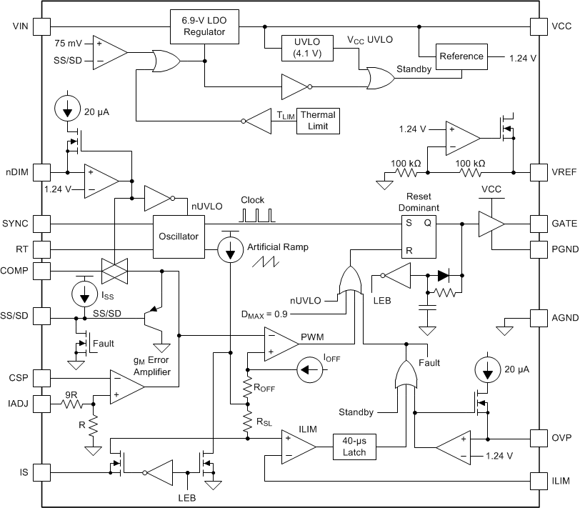
7.2 Functional Block Diagram
7.3 Feature Description
7.3.1 Current Regulators
Current regulators can be designed to accomplish different functions: boost, buck-boost, and flyback. The TPS92690 device is designed to drive a ground referenced N-channel FET and sense a ground referenced LED load. This control architecture is perfect for driving boost, SEPIC, flyback, or Cuk topologies. It does not work with a floating buck or buck-boost topology since the LED current sense amplifier is ground referenced.
Looking at the boost design in the Typical Boost Application, the basic operation of a current regulator can be analyzed. During the time that the N-channel FET (Q1) is turned on (tON), the input voltage source stores energy in the inductor (L1) while the output capacitor (CO) provides energy to the LED load. When Q1 is turned off (tOFF), the re-circulating diode (D1) becomes forward biased and L1 provides energy to both CO and the LED load. Figure 11 shows the inductor current (iL(t)) waveform for a regulator operating in CCM.
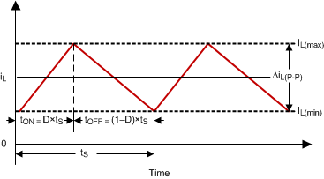 Figure 11. Basic CCM Inductor Current Waveform
The average output LED current (ILED) is proportional to the average inductor current (IL), therefore if IL is tightly controlled, ILED is well regulated. As the system changes input voltage or output voltage, the ideal duty cycle (D) is varied to regulate IL and ultimately ILED. For any current regulator, D is a function of the conversion ratio:
Use Equation 1 to calculate the duty cycle for an application using the boost topology.

Use Equation 2 to calculate the duty cycle for an application using the buck-boost (SEPIC/Cuk) topology.

Use Equation 3 to calculate the duty cycle for an application using the flyback topology.

where
- n is the primary to secondary turns ratio of the coupled inductor, n:1
7.3.2 Peak Current Mode Control
Peak current mode control is used by the TPS92690 device to regulate the average LED current through an array of HBLEDs. This method of control uses a series resistor in the LED path to sense LED current and can use either a series resistor in the MOSFET path or the MOSFET RDS(on) for both cycle-by-cycle current limit and input voltage feed forward. The controller has a fixed switching frequency set by an internal programmable oscillator therefore slope compensation is added to mitigate current mode instability. A detailed explanation of this control method is presented in the following sections.
7.3.3 Switching Frequency and Synchronization
The switching frequency of the TPS92690 device is programmed using an external resistor (RT) connected from the RT pin to GND. This switching frequency is defined as shown in Equation 4.

The Typical Characteristics shows a graph of switching frequency versus timing resistance on RT. For maximum operational range and best efficiency, TI recommends a switching frequency of 1 MHz or lower. It is possible to reduce the solution size in applications with switching frequencies as high as 2 MHz in some situations. Higher frequencies require an increased gate-drive current and that can result in higher AC losses, both of which result in decreased efficiency. It is also possible that the minimum on-time (leading edge blanking time) limits the minimum operational duty cycle and reduces the input voltage range for a given output voltage.
Alternatively, an external PWM signal can be applied to the SYNC pin to synchronize the device to an external clock. If the PWM signal frequency applied is higher than the base frequency set by the timing (RT) resistor, the internal oscillator is bypassed and the switching frequency is equal to the synchronized frequency. The PWM signal should have an amplitude between 2.5 and 5 V. The device triggers a switch-on time on the falling edge of the PWM signal and operates correctly regardless of the duty cycle of the applied signal.
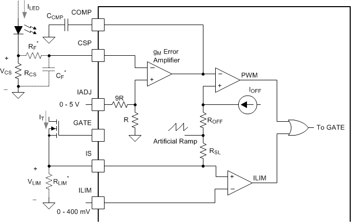 Figure 12. Current Sense and Control Circuitry (* optional)
7.3.4 Current Sense and Current Limit
The TPS92690 device implements peak current mode control using the circuit shown in Figure 12. The peak detection is accomplished with a comparator that monitors the main MOSFET current, comparing it with the COMP pin. When the IS pin voltage (plus the DC level shift and the ramp discussed later) exceeds the COMP pin voltage, the MOSFET is turned off. The MOSFET is turned back on when the oscillator starts a new on-time and the cycle repeats.
The IS pin incorporates a cycle-by-cycle overcurrent protection function. Current limit is accomplished by a redundant internal current sense comparator. If the voltage at the current sense comparator input (IS) exceeds the voltage at the ILIM pin, the MOSFET is turned off and the COMP pin is pulled to ground and discharged. The MOSFET turns back on after either the 43-µs current limit timeout has passed or after the COMP pin is recharged, whichever is longer. The IS input pin has an internal N-channel MOSFET which pulls it down at the conclusion of every cycle. The discharge device remains on an additional 216 ns (typical) after the beginning of a new cycle to blank the leading edge spike on the current sense signal. This blanking time also results in a minimum switch-on time of 216 ns which determines a minimum duty cycle dependent upon switching frequency.
IS sensing can be done in one of two ways. The most accurate current sensing is accomplished by using a resistor, RLIM. This adds a component that dissipates additional power but the result is higher accuracy and no limitation on the maximum MOSFET drain voltage. For applications that have a maximum MOSFET drain voltage below 75 V MOSFET RDS(on) sensing can be used by connecting the IS pin directly to the drain of the MOSFET and eliminating RLIM. This results in higher efficiency but the accuracy depends on the accuracy of the MOSFET RDS(on). Care must be taken to use the maximum expected RDS(on) when setting the current limit threshold at the ILIM pin.
7.3.5 Average LED Current
The COMP pin voltage is dynamically adjusted, via the internal error amplifier, to maintain the desired regulation. A sense resistor in series with the LEDs sets the average LED current regulation. The voltage across the sense resistor (VCS) is regulated to the IADJ voltage divided by 10.
The IADJ pin can be set to any value up to 2.45 V by connecting it to VREF through a resistor divider for static output current settings. IADJ can also be used to change the regulation point if connected to a controlled voltage source up to 5 V or potentiometer to provide analog dimming. It is also possible to configure the IADJ pin for thermal foldback functions.


The TPS92690 device maintains high accuracy at any level of VCS. However, the accuracy remains better with higher levels as offsets and other errors become a smaller percentage of the overall VCS voltage. Power losses are also higher with higher VCS voltages. A good tradeoff for accuracy and efficiency is to set the maximum VCS voltage to between 100 and 250 mV.
In some applications, such as standard boost or flyback topologies, the output capacitor can be connected from the output directly to ground. In these cases the CS pin can be directly connected to RCS. In other applications an additional filter may be desired on the CS pin (RF and CF). Use these filters with topologies where the current through RCS is not continuous such as in the Cuk configuration. Another example would be a boost regulator where PWM dimming is required and the output capacitor is connected directly across the LEDs. In these cases it is recommended to add a 47-Ω resistor for RF and a 47-nF capacitor for CF to achieve the best accuracy and line regulation.
7.3.6 Precision Reference (VREF)
The TPS92690 device includes a precision 2.45-V reference. This can be used in conjunction with a resistor divider to set voltage levels for the ILIM pin and the IADJ pin to set the maximum current limit and LED current. It can also be used with high impedance external circuitry requiring a reference. To set the current limit (ICL) using VREF you can use the following equations:


When RDS(on) sensing is being used substitute RLIM in the above equation with RDS(on). A small amount of capacitance (CLIM) can be placed from the ILIM pin to ground for filtering if desired. If so, a value between 47 pF and 100 nF should be used but this value should not exceed the value of CCMP to avoid false triggering of the current limit. To set the IADJ voltage level using VREF use the following equation:

If desired, place a small capacitor (CADJ) from the IADJ pin to ground for additional filtering. A value between 47 pF and 100 nF should be sufficient.
7.3.7 Low-Level Analog Dimming
The IADJ pin can be driven as low as 0 V. The device encounters a minimum on-time at some level, depending on the switching frequency. When the voltage on the IADJ pin falls beyond this point, the device begins to skip pulses to maintain average output current regulation. Depending on external components and regulator bandwidth this skipping may or may not result in visible flicker. If flicker is present below this level higher inductor and/or output capacitor values may help and a lower COMP pin capacitor value may help. In many cases this level occurs at very low LED current and it is more desirable to simply limit the low level on the IADJ pin as shown in Figure 13.
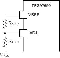 Figure 13. Limiting Minimum IADJ Voltage
The resulting IADJ voltage can be found using the following equation:

7.3.8 Soft-Start and Shutdown
The TPS92690 device can be placed into low power shutdown by grounding the SS/SD pin (any voltage below 86 mV). During low power shutdown, the device limits the quiescent current to approximately 40 µA, typical.
The SS/SD pin also has a 10-µA current source (or 1 µA when below the 86-mV shutdown threshold), which charges a capacitor from SS/SD to GND to soft-start the converter. The SS/SD pin is attached through a PNP transistor to COMP therefore it controls the speed at which COMP rises at startup. When VCCUV is below the falling threshold, SS/SD is pulled down to reset the capacitor voltage to zero. Then when VCCUV rising threshold is exceeded, the pin is released and charges via the 10-µA current source.
7.3.9 VCC Regulator and Start-Up
The TPS92690 device includes a high voltage, low dropout bias regulator. When power is applied, or SS/SD is released, the regulator is enabled and sources current into an external capacitor (CBYP) connected to the VCC pin. The recommended bypass capacitance for the VCC regulator is 2.2 to 3.3 µF. This capacitor should be rated for 10 V or greater and an X7R dielectric ceramic is recommended. The output of the VCC regulator is monitored by an internal UVLO circuit that protects the device from attempting to operate with insufficient supply voltage and the supply is also internally current limited. VCC may also be driven externally to increase the GATE voltage and reduce the RDS(on) of the external switching MOSFET. The maximum voltage on this pin is 14 V and should not exceed the VIN voltage. The bypass capacitor voltage rating may need to be increased accordingly.
The start-up time of the device to full output current depends on the value of CBYP, CSS (soft-start capacitor), CCMP, and CO (output capacitor) as shown in Figure 14:
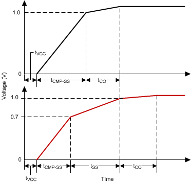 Figure 14. Start-up Waveforms
First, CBYP is charged to be above the VCC UVLO threshold of 4.1 V. The CBYP charging time (tVCC) can be estimated as:

Assuming there is no CSS (top trace), or if CSS is less than 40% of CCMP, CCMP is then charged to 1V over the charging time (tCMP) which can be estimated as:

Once CCMP = 1 V, the device starts switching to charge CO until the LED current is in regulation. The CO charging time (tCO) can be roughly estimated as:

If CSS is greater than 40% of CCMP (bottom trace), the compensation capacitor only charges to 0.7 V over a smaller CCMP charging time (tCMP-SS) which can be estimated as:

Then COMP clamps to SS, forcing COMP to rise (the last 300 mV before switching begins) according to the CSS charging time (tSS) which can be estimated as:

The system start-up time tSU (for CSS < 0.4 CCMP) or tSU-SS (for CSS > 0.4 CCMP) is defined as:


As a general rule of thumb, standard smooth startup operation can be achieved with CSS = CCMP. If SD/SS is being driven by an external source the equations above may need to be modified depending on the current sourcing capability of the external source.
7.3.10 Overvoltage Protection (OVP)
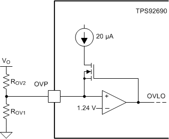 Figure 15. Overvoltage Protection Circuitry
The TPS92690 device includes a dedicated OVP pin which can be used for either input or output over-voltage protection. This pin features a precision 1.24-V threshold with 20 µA (typical) of hysteresis current as shown in Figure 15. When the OVP threshold is exceeded, the GATE pin is immediately pulled low and a 20-µA current source provides hysteresis to the lower threshold of the OVP hysteretic band.
The over-voltage turn-off threshold (VTURN-OFF) and the hysteresis (VHYSO) are defined by:


7.3.11 Input Undervoltage Lockout (UVLO)
The nDIM pin is a dual function input that features an accurate 1.24-V threshold with programmable hysteresis as shown in Figure 16. This pin functions as both the PWM dimming input for the LEDs and as a VIN UVLO. When the pin voltage rises and exceeds the 1.24-V threshold, 20 µA (typical) of current is driven out of the nDIM pin into the resistor divider providing programmable hysteresis.
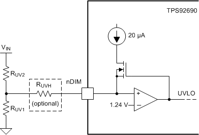 Figure 16. UVLO Circuit
When using the nDIM pin for UVLO and PWM dimming concurrently, the UVLO circuit can have an extra resistor to set the hysteresis. This allows the standard resistor divider to have smaller values minimizing PWM delays due to a pull-down MOSFET at the nDIM pin (see PWM Dimming). In general, at least 3 V of hysteresis is preferable when PWM dimming if operating near the UVLO threshold. The turn-on threshold (VTURN-ON) is defined as follows:

The hysteresis (VHYS) is defined as follows:
UVLO Only

PWM Dimming and UVLO

7.3.12 PWM Dimming
The active low nDIM pin can be driven with a PWM signal which controls the main N-channel FET. The brightness of the LEDs can be varied by modulating the duty cycle of this signal. LED brightness is approximately proportional to the PWM signal duty cycle (that is, 30% nDIM high duty cycle equals about 30% LED brightness). This function can be ignored if PWM dimming is not required by using nDIM solely as a VIN UVLO input as described in the Input Undervoltage Lockout (UVLO) section or by tying it directly to VCC or VIN when UVLO is not required.
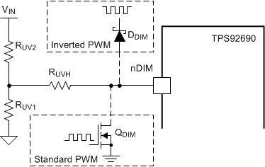 Figure 17. PWM Dimming Circuit
When using a MOSFET (QDIM), connect the drain to the nDIM pin and the source to GND. Apply an external logic-level PWM signal to the gate of QDIM. Brightness is proportional to the negative duty cycle of the PWM signal. When using a Schottky diode (DDIM), connect the anode to the nDIM pin. Apply an external logic-level PWM signal to the cathode of the diode and brightness is proportional to the positive duty cycle of the PWM signal.
7.3.13 Control Loop Compensation
Compensating the TPS92690 device is relatively simple for most applications. To prevent subharmonic oscillations due to current mode control, a minimum inductor value should be chosen. This minimum value can be approximated with the following equation:

Compensating the control loop simply requires a capacitor from the COMP pin to ground. Most LED driver applications do not require high bandwidth response since there are no significant output transients and generally limited, low bandwidth input transients. The high output impedance (RO) of the error amplifier (typically 200MΩ) enables a low bandwidth system where standard poles and zeros, including the right half plane zero in many cases, can be neglected. In this case the bandwidth of the system generally becomes the bandwidth of the error amplifier. TI recommends a CCMP value of 1 to 100 nF, which results in the following dominant pole and crossover frequency:


A 1-nF capacitor results in a bandwidth of approximately 5.2 kHz while a 100-nF capacitor results in a bandwidth of approximately 52 Hz. Larger values are recommended for most applications unless higher bandwidth is required. Larger values are also recommended for applications requiring PWM dimming as it allows the COMP pin to hold its level more accurately during the LED current off time. In applications where the duty cycle (D) exceeds 0.5 (VIN < VO / 2 for a boost regulator) the location of the right half plane zero should be calculated to ensure stability using the following equation:

Where D and D’ are calculated using the minimum input voltage. The crossover frequency, ƒC, should be a decade below ƒRHPZ for maximum stability. CCMP should be adjusted accordingly if required.
7.3.14 Thermal Shutdown
The TPS92690 device includes thermal shutdown protection. If the die temperature reaches approximately 175°C the device shuts down (GATE pin low). If the die temperature is allowed to cool until it reaches approximately 150°C the device resumes normal operation.
7.4 Device Functional Modes
This device has no additional functional modes