ZHCSPL6 January 2022 TPS7H4003-SEP
PRODUCTION DATA
- 1 特性
- 2 应用
- 3 说明
- 4 Revision History
- 5 Pin Configuration and Functions
- 6 Specifications
-
7 Detailed Description
- 7.1 Overview
- 7.2 Functional Block Diagram
- 7.3
Feature Description
- 7.3.1 VIN and Power VIN Pins (VIN and PVIN)
- 7.3.2 Voltage Reference
- 7.3.3 Adjusting the Output Voltage
- 7.3.4 Safe Start-Up Into Prebiased Outputs
- 7.3.5 Error Amplifier
- 7.3.6 Enable and Adjust UVLO
- 7.3.7 Adjustable Switching Frequency and Synchronization (SYNC)
- 7.3.8 Soft-Start (SS/TR)
- 7.3.9 Power Good (PWRGD)
- 7.3.10 Sequencing
- 7.3.11 Output Overvoltage Protection (OVP)
- 7.3.12 Overcurrent Protection
- 7.3.13 Thermal Shutdown
- 7.3.14 Turn-On Behavior
- 7.3.15 Slope Compensation
- 7.3.16 Small Signal Model for Frequency Compensation
- 7.4 Device Functional Modes
-
8 Application and Implementation
- 8.1 Application Information
- 8.2
Typical Application
- 8.2.1 Design Requirements
- 8.2.2
Detailed Design Procedure
- 8.2.2.1 Operating Frequency
- 8.2.2.2 Output Inductor Selection
- 8.2.2.3 Output Capacitor Selection
- 8.2.2.4 Output Schottky Diode
- 8.2.2.5 Input Capacitor Selection
- 8.2.2.6 Soft-Start Capacitor Selection
- 8.2.2.7 Undervoltage Lockout (UVLO) Set Point
- 8.2.2.8 Output Voltage Feedback Resistor Selection
- 8.2.2.9 Compensation Component Selection
- 8.2.3 Parallel Operation
- 8.2.4 Application Curve
- 9 Power Supply Recommendations
- 10Layout
- 11Device and Documentation Support
- 12Mechanical, Packaging, and Orderable Information
8.2.2.2 Output Inductor Selection
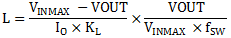
To calculate the value of the output inductor, use Equation 23. KL is a coefficient that represents the amount of inductor ripple current relative to the maximum output current, IO as shown in Equation 14. The inductor ripple current is filtered by the output capacitor, therefore, choosing high inductor ripple currents impact the selection of the output capacitor since the output capacitor must have a ripple current rating equal to or greater than the inductor ripple current. In general, the inductor ripple value is at the discretion of the designer depending on specific system needs. Typical values for KL range from 0.1 to 0.5. For low output currents, the value of KL could be increased to reduce the value of the output inductor.
For this design example, use KL = 0.1 and the inductor value is calculated to be 0.9 µH for nominal VIN = 5 V.
For the output filter inductor, it is important that the RMS current and saturation current ratings not be exceeded. The RMS and peak inductor current can be found from Equation 25 and Equation 26.


For this design, the RMS inductor current is 18 A and the peak inductor current is 18.9 A. In order to satisfy all requirements, a 1-μH Coilcraft XAL1580 inductor was used.
The current flowing through the inductor is the inductor ripple current plus the output current. During power up, faults or transient load conditions, the inductor current can increase above the calculated peak inductor current level calculated previously. In transient conditions, the inductor current can increase up to the switch current limit of the device. For this reason, the most conservative approach is to specify an inductor with a saturation current rating equal to or greater than the switch current limit rather than the peak inductor current.