ZHCSOO0C september 2021 – june 2023 TPS7A94
PRODUCTION DATA
- 1
- 1 特性
- 2 应用
- 3 说明
- 4 Revision History
- 5 Pin Configuration and Functions
- 6 Specifications
-
7 Detailed Description
- 7.1 Overview
- 7.2 Functional Block Diagram
- 7.3
Feature Description
- 7.3.1 Output Voltage Setting and Regulation
- 7.3.2 Ultra-Low Noise and Ultra-High Power-Supply Rejection Ratio (PSRR)
- 7.3.3 Programmable Current Limit and Power-Good Threshold
- 7.3.4 Programmable Soft Start (NR/SS Pin)
- 7.3.5 Precision Enable and UVLO
- 7.3.6 Active Discharge
- 7.3.7 Thermal Shutdown Protection (TSD)
- 7.4 Device Functional Modes
-
8 Application and Implementation
- 8.1
Application Information
- 8.1.1 Output Voltage Restart (Overshoot Prevention Circuit)
- 8.1.2 Precision Enable (External UVLO)
- 8.1.3 Undervoltage Lockout (UVLO) Operation
- 8.1.4 Dropout Voltage (VDO)
- 8.1.5 Power-Good Feedback (FB_PG Pin) and Power-Good Threshold (PG Pin)
- 8.1.6 Adjusting the Factory-Programmed Current Limit
- 8.1.7 Programmable Soft-Start and Noise-Reduction (NR/SS Pin)
- 8.1.8 Inrush Current
- 8.1.9 Optimizing Noise and PSRR
- 8.1.10 Adjustable Operation
- 8.1.11 Paralleling for Higher Output Current and Lower Noise
- 8.1.12 Recommended Capacitor Types
- 8.1.13 Load Transient Response
- 8.1.14 Power Dissipation (PD)
- 8.1.15 Estimating Junction Temperature
- 8.1.16 TPS7A94EVM-046 Thermal Analysis
- 8.2 Typical Application
- 8.3 Power Supply Recommendations
- 8.4 Layout
- 8.1
Application Information
- 9 Device and Documentation Support
- 10Mechanical, Packaging, and Orderable Information
8.2.2 Detailed Design Procedure
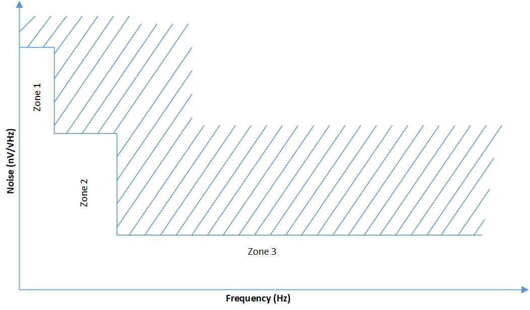
In this design example, the device is powered by a dc/dc convertor switching at 1 MHz. The load requires a 3.3-V clean rail with the spectral noise mask versus frequency shown in Figure 8-29 and a maximum load of 500 mA. The typical 10-μF input and output capacitors and 4.7-μF NR/SS capacitors are used to achieve a good balance between fast start-up time and excellent noise and PSRR performance.
 Figure 8-29 Noise Compliance Mask
The output voltage is set using a 22.1-kΩ, thin-film resistor value calculated as described in the Adjustable Operation section. To set the current limit to a value close to the 750 mA required by the application, and to set the PG threshold to 95%, use Table 8-2 to set the RFB_PG top and bottom resistors values at 1.47 MΩ and 100 kΩ, respectively.
Setting RB to 100 kΩ and using a 4-V VON and Equation 1 provide the RT value of 226 kΩ. VOFF is calculated with Equation 2 to be 3.5 V.
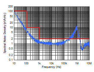
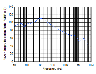
Figure 8-30 shows that the device meets all design noise requirements except for the noise peaking at 900 kHz. However, this noise peaking can be easily attenuated to the required noise level by means of a pi-filter positioned after the LDO. Figure 8-31 shows that this design is very close to the PSRR level at 1 MHz and can require more margin. Fortunately, both requirements are easily achieved by inserting a pi-filter consisting of a ferrite bead and a small capacitor beyond the LDO and before the load; see Figure 8-28.
The ferrite bead was selected to have a very small dc resistance of less than 50 mΩ, 1 A of current rating, and a relatively small footprint. The added pi-filter components have almost no impact on the LDO accuracy performance and no significant increase in the design total cost.
 Figure 8-30 Output Noise vs
Frequency
 Figure 8-31 PSRR vs Frequency