ZHCSOO0C september 2021 – june 2023 TPS7A94
PRODUCTION DATA
- 1
- 1 特性
- 2 应用
- 3 说明
- 4 Revision History
- 5 Pin Configuration and Functions
- 6 Specifications
-
7 Detailed Description
- 7.1 Overview
- 7.2 Functional Block Diagram
- 7.3
Feature Description
- 7.3.1 Output Voltage Setting and Regulation
- 7.3.2 Ultra-Low Noise and Ultra-High Power-Supply Rejection Ratio (PSRR)
- 7.3.3 Programmable Current Limit and Power-Good Threshold
- 7.3.4 Programmable Soft Start (NR/SS Pin)
- 7.3.5 Precision Enable and UVLO
- 7.3.6 Active Discharge
- 7.3.7 Thermal Shutdown Protection (TSD)
- 7.4 Device Functional Modes
-
8 Application and Implementation
- 8.1
Application Information
- 8.1.1 Output Voltage Restart (Overshoot Prevention Circuit)
- 8.1.2 Precision Enable (External UVLO)
- 8.1.3 Undervoltage Lockout (UVLO) Operation
- 8.1.4 Dropout Voltage (VDO)
- 8.1.5 Power-Good Feedback (FB_PG Pin) and Power-Good Threshold (PG Pin)
- 8.1.6 Adjusting the Factory-Programmed Current Limit
- 8.1.7 Programmable Soft-Start and Noise-Reduction (NR/SS Pin)
- 8.1.8 Inrush Current
- 8.1.9 Optimizing Noise and PSRR
- 8.1.10 Adjustable Operation
- 8.1.11 Paralleling for Higher Output Current and Lower Noise
- 8.1.12 Recommended Capacitor Types
- 8.1.13 Load Transient Response
- 8.1.14 Power Dissipation (PD)
- 8.1.15 Estimating Junction Temperature
- 8.1.16 TPS7A94EVM-046 Thermal Analysis
- 8.2 Typical Application
- 8.3 Power Supply Recommendations
- 8.4 Layout
- 8.1
Application Information
- 9 Device and Documentation Support
- 10Mechanical, Packaging, and Orderable Information
8.1.10 Adjustable Operation
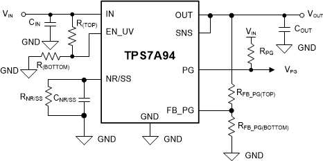
As shown in Figure 8-16, the output voltage of the device can be set using a single external resistor (RNR/SS). Equation 6 calculates the output voltage.
 Figure 8-16 Typical
Circuit
Figure 8-16 Typical
CircuitTable 8-4 shows the recommended RNR/SS resistor values to achieve several common rails using a standard 1%-tolerance resistor.
| TARGETED OUTPUT VOLTAGE (V) |
RNR/SS (kΩ) | CALCULATED OUTPUT VOLTAGE (V) |
|---|---|---|
| 0.4 | 2.67 | 0.4005 |
| 0.5 | 3.32 | 0.498 |
| 0.6 | 4.02 | 0.603 |
| 0.7 | 4.64 | 0.696 |
| 0.8 | 5.36 | 0.804 |
| 0.9 | 6.04 | 0.906 |
| 1.0 | 6.65 | 0.9975 |
| 1.2 | 8.06 | 1.209 |
| 1.5 | 10.0 | 1.5 |
| 2.5 | 16.5 | 2.475 |
| 3.0 | 20.0 | 3.0 |
| 3.3 | 22.1 | 3.315 |
| 3.6 | 24.3 | 3.645 |
| 4.7 | 31.6 | 4.74 |
| 5.0 | 33.2 | 4.98 |
To avoid engaging the current limit during start-up with a large COUT capacitor, make sure that:
- A minimum NR/SS capacitor of 1 μF is used
- When the output capacitor is greater than 100 μF, maintain a COUT to CNR/SS ratio < 100
Because the set resistor is also placed on the NR/SS pin, consider using a thin-film resistor and provide enough resistor temperature drift to ensure the targeted accuracy.