ZHCSEP4A January 2016 – February 2016 TPS7A85
PRODUCTION DATA.
- 1 特性
- 2 应用
- 3 说明
- 4 修订历史记录
- 5 Pin Configurations and Functions
- 6 Specifications
- 7 Detailed Description
-
8 Application and Implementation
- 8.1
Application Information
- 8.1.1 Recommended Capacitor Types
- 8.1.2 Input and Output Capacitor Requirements (CIN and COUT)
- 8.1.3 Noise-Reduction and Soft-Start Capacitor (CNR/SS)
- 8.1.4 Feed-Forward Capacitor (CFF)
- 8.1.5 Soft-Start and In-Rush Current
- 8.1.6 Optimizing Noise and PSRR
- 8.1.7 ANY-OUT Programmable Output Voltage
- 8.1.8 ANY-OUT Operation
- 8.1.9 Increasing ANY-OUT Resolution for LILO Conditions
- 8.1.10 Current Sharing
- 8.1.11 Adjustable Operation
- 8.1.12 Sequencing Requirements
- 8.1.13 Power-Good (PG) Operation
- 8.1.14 Undervoltage Lockout (UVLO) Operation
- 8.1.15 Dropout Voltage (VDO)
- 8.1.16 Behavior when Transitioning from Dropout into Regulation
- 8.1.17 Load Transient Response
- 8.1.18 Negatively-Biased Output
- 8.1.19 Reverse Current Protection
- 8.1.20 Power Dissipation (PD)
- 8.2 Typical Applications
- 8.1
Application Information
- 9 Power-Supply Recommendations
- 10Layout
- 11器件和文档支持
- 12机械、封装和可订购信息
8 Application and Implementation
NOTE
Information in the following applications sections is not part of the TI component specification, and TI does not warrant its accuracy or completeness. TI’s customers are responsible for determining suitability of components for their purposes. Customers should validate and test their design implementation to confirm system functionality.
8.1 Application Information
The TPS7A85 is a linear voltage regulator with an input voltage range of 1.1 V to 6.5 V and an output voltage range of 0.8 V to 5.0 V with a 1% accuracy and a 4-A maximum output current. The TPS7A85 has an integrated charge pump for ease of use and an external bias rail to allow for the lowest dropout across the entire output voltage range.
8.1.1 Recommended Capacitor Types
The TPS7A85 is designed to be stable using low equivalent series resistance (ESR) ceramic capacitors at the input, output, and noise-reduction pin (NR, pin 13). Multilayer ceramic capacitors have become the industry standard for these types of applications and are recommended, but must be used with good judgment. Ceramic capacitors that employ X7R-, X5R-, and COG-rated dielectric materials provide relatively good capacitive stability across temperature, whereas the use of Y5V-rated capacitors is discouraged because of large variations in capacitance.
Regardless of the ceramic capacitor type selected, ceramic capacitance varies with operating voltage and temperature. As a rule of thumb, derate ceramic capacitors by at least 50%. The input and output capacitors recommended herein account for a effective capacitance derating of approximately 50%, but at high VIN and VOUT conditions (that is, VIN = 5.5 V to VOUT = 5.0 V) the derating can be greater than 50% and must be taken into consideration.
8.1.2 Input and Output Capacitor Requirements (CIN and COUT)
The TPS7A85 is designed and characterized for operation with ceramic capacitors of 47 µF or greater (22 μF or greater of effective capacitance) at the output and 10 µF or greater (5 μF or greater of effective capacitance) at the input. Using at least a 47-µF capacitor is highly recommended at the input to minimize input impedance. Place the input and output capacitors as near as practical to the respective input and output pins to minimize trace parasitics. If the trace inductance from the input supply to the TPS7A85 is high, a fast current transient can cause VIN to ring above the absolute maximum voltage rating and damage the device. This situation can be mitigated by additional input capacitors to dampen the ringing and to keep the ringing below the device absolute maximum ratings.
A combination of multiple output capacitors boosts the high-frequency PSRR, as illustrated in several of the PSRR curves. The combination of one 0805-sized, 47-µF ceramic capacitor in parallel with two 0805-sized,
10-µF ceramic capacitors with a sufficient voltage rating in conjunction with the PSRR boost circuit optimizes PSRR for the frequency range of 400 kHz to 700 kHz (which is a typical range for dc-dc supply switching frequency). This 47-µF || 10-µF || 10-µF combination also ensures that at high input voltage and high output voltage configurations, the minimum effective capacitance is met. Many 0805-sized, 47-µF ceramic capacitors have a voltage derating of approximately 60% to 75% at 5.0 V, so the addition of the two 10-µF capacitors ensures that the capacitance is at or above 22 µF.
8.1.3 Noise-Reduction and Soft-Start Capacitor (CNR/SS)
The TPS7A85 features a programmable, monotonic, voltage-controlled soft-start that is set with an external capacitor (CNR/SS).The use of an external CNR/SS is highly recommended, especially to minimize in-rush current into the output capacitors. This soft-start eliminates power-up initialization problems when powering field-programmable gate arrays (FPGAs), digital signal processors (DSPs), or other processors. The controlled voltage ramp of the output also reduces peak in-rush current during start-up, minimizing start-up transients to the input power bus.
To achieve a monotonic start-up, the TPS7A85 error amplifier tracks the voltage ramp of the external soft-start capacitor until the voltage approaches the internal reference. The soft-start ramp time depends on the soft-start charging current (INR/SS), the soft-start capacitance (CNR/SS), and the internal reference (VNR/SS). Soft-start ramp time can be calculated with Equation 1:
Note that INR/SS is provided in the Electrical Characteristics table and has a typical value of 6.2 µA.
The noise-reduction capacitor, in conjunction with the noise-reduction resistor, forms a low-pass filter (LPF) that filters out the noise from the reference before being gained up with the error amplifier, thereby reducing the device noise floor. The LPF is a single-pole filter and the cutoff frequency can be calculated with Equation 2. The typical value of RNR is 250 kΩ. Increasing the CNR/SS capacitor has a greater affect because the output voltage increases when the noise from the reference is gained up even more at higher output voltages. For low-noise applications, a 10-nF to 1-µF CNR/SS is recommended.
8.1.4 Feed-Forward Capacitor (CFF)
Although a feed-forward capacitor (CFF) from the FB pin to the OUT pin is not required to achieve stability, a
10-nF external feed-forward capacitor optimizes the transient, noise, and PSRR performance. A higher capacitance CFF can be used; however, the start-up time is longer and the power-good signal can incorrectly indicate that the output voltage is settled. To ensure proper PG functionality the time constant defined by CNR/SS must be greater than or equal to the time constant from the CFF. For a detailed description, see application report Pros and Cons of Using a Feed-Forward Capacitor with a Low Dropout Regulator, SBVA042.
8.1.5 Soft-Start and In-Rush Current
Soft-start refers to the ramp-up characteristic of the output voltage during LDO turn-on after EN and both UVLOs exceed their threshold voltages. The noise-reduction capacitor serves a dual purpose of both governing output noise reduction and programming the soft-start ramp during turn-on.
The soft-start ramp is not fully linear as the error amplifier has a several millivolt offset voltage. The output voltage starts to ramp only after the voltage created by the soft-start circuit increases above this offset voltage, at which point the output rises quickly to the voltage on the NR/SS pin. After this initial jump, the voltage rises at the ramp rate determined by the soft-start function. This jump typically does not cause a problem in applications because the quick rise in the output voltage has a very small amplitude.
In-rush current is defined as the current into the LDO at the IN pin during start-up. In-rush current then consists primarily of the sum of load current and the current used to charge the output capacitor. This current is difficult to measure because the input capacitor must be removed, which is not recommended. However, this soft-start current can be estimated by Equation 3:

where
- VOUT(t) is the instantaneous output voltage of the turn-on ramp
- dVOUT(t) / dt is the slope of the VOUT ramp
- RLOAD is the resistive load impedance
8.1.6 Optimizing Noise and PSRR
The ultra-low noise floor and PSRR of the device can be improved by careful selection of:
- CNR/SS for the low-frequency range
- CFF for the mid-band frequency range
- COUT for the high-frequency range
- VIN – VOUT for all frequencies, and
- VBIAS at lower input voltages
The noise-reduction capacitor filters out low-frequency noise from the reference and the feed-forward capacitor reduces output voltage noise by filtering out the mid-band frequency noise. However, a large feed-forward capacitor can create some new issues that are discussed in application report Pros and Cons of Using a Feed-Forward Capacitor with a Low Dropout Regulator, SBVA042.
Note that a large output capacitor reduces high-frequency output voltage noise. Additionally, a bias rail or higher input voltage improves the noise because greater headroom is provided for the internal circuits. A high power dissipation across the die increases the output noise because of the increase in junction temperature.
A larger noise-reduction capacitor improves low-frequency PSRR by filtering any noise coupling from the input into the reference. The feed-forward capacitor can be optimized by placing a pole-zero pair near the edge of the loop bandwidth and pushing out the loop bandwidth, thus improving mid-band PSRR. Larger output capacitors and various output capacitors can be used to improve high-frequency PSRR; see Figure 7 for more details.
A higher input voltage improves PSRR by providing the device more headroom to respond to noise on the input; see Figure 2. A bias rail also improves the PSRR at lower input voltages because greater headroom is provided for the internal circuits. Table 1 lists the output voltage noise for the 10-Hz to 100-kHz band at a 5.0-V output for a variety of conditions with an input voltage of 5.6 V, an R1 of 12.1 kΩ, and a load current of 4 A. The 5.0-V output is chosen because this output is the worst-case condition for output voltage noise. Note that the input voltage is 5.6 V, not 5.5 V as provided in the Electrical Characteristics table. The higher input voltage limits the maximum ambient temperature to below 40°C on a standard-JEDEC high-K board; see the Power Dissipation (PD) section for more information.
Table 1. Output Noise Voltage at a 5.0-V Output with a 5.6-V Input
| CNR/SS (nF) | CFF (nF) | COUT (µF) | OUTPUT VOLTAGE NOISE (µVRMS) |
|---|---|---|---|
| 10 | 10 | 47 || 10 || 10 | 12.3 |
| 100 | 10 | 47 || 10 || 10 | 8.4 |
| 100 | 100 | 47 || 10 || 10 | 6.6 |
| 100 | 100 | 1000 | 6.4 |
8.1.6.1 Charge Pump Noise
The device internal charge pump generates a minimal amount of noise, as shown in Figure 46.
Using a bias rail minimizes the internal charge pump noise when the internal voltage is clamped, thereby reducing the overall output noise floor.
The high-frequency components of the output voltage noise density curve are filtered out in most applications by using 10-nF to 100-nF bypass capacitors close to the load. Using a ferrite bead between the LDO output and the load input capacitors forms a pi-filter, further reducing the high-frequency noise contribution.
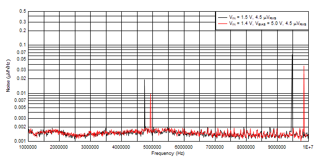 Figure 46. Charge Pump Noise
8.1.7 ANY-OUT Programmable Output Voltage
The TPS7A85 can either use external resistors or the internally-matched ANY-OUT feedback resistor network to set the output voltage. The ANY-OUT resistors are accessible via pins 2 and 5 to 11 and are used to program the regulated output voltage. Each pin can be connected to ground (active) or left open (floating), or connected to SNS. ANY-OUT programming is set by Equation 4 as the sum of the internal reference voltage (VNR/SS = 0.8 V) plus the accumulated sum of the respective voltages assigned to each active pin; that is, 50mV (pin 5), 100mV (pin 6), 200mV (pin 7), 400mV (pin 9), 800mV (pin 10), or 1.6V (pin 11). Table 2 summarizes these voltage values associated with each active pin setting for reference. By leaving all program pins open or floating, the output is thereby programmed to the minimum possible output voltage equal to VFB.
Table 2. ANY-OUT Programmable Output Voltage
| ANY-OUT PROGRAM PINS (Active Low) | ADDITIVE OUTPUT VOLTAGE LEVEL |
|---|---|
| Pin 5 (50mV) | 50 mV |
| Pin 6 (100mV) | 100 mV |
| Pin 7 (200mV) | 200 mV |
| Pin 9 (400mV) | 400 mV |
| Pin 10 (800mV) | 800 mV |
| Pin 11 (1.6V) | 1.6 V |
Table 3 provides a full list of target output voltages and corresponding pin settings when the ANY-OUT pins are only tied to ground or left floating. The voltage setting pins have a binary weight; therefore, the output voltage can be programmed to any value from 0.8 V to 3.95 V in 50-mV steps when tying these pins to ground. There are several alternative ways to set the output voltage. The program pins can be driven by using external general-purpose input/output pins (GPIOs), manually connected using 0-Ω resistors (or left open), or hardwired by the given layout of the printed circuit board (PCB) to set the ANY-OUT voltage. As with the adjustable operation, the output voltage is set according to Equation 5 except that R1 and R2 are internally integrated and matched for higher accuracy. Tying any of the ANY-OUT pins to SNS can increase the resolution of the internal feedback network by lowering the value of R1; see the Increasing ANY-OUT Resolution for LILO Conditions section for additional information.
NOTE
For output voltages greater than 3.95 V, use a traditional adjustable configuration (see the Adjustable Operation section).
Table 3. User-Configurable Output Voltage Settings
| VOUT(NOM)
(V) |
50mV | 100mV | 200mV | 400mV | 800mV | 1.6V | VOUT(NOM)
(V) |
50mV | 100mV | 200mV | 400mV | 800mV | 1.6V | |
|---|---|---|---|---|---|---|---|---|---|---|---|---|---|---|
| 0.80 | Open | Open | Open | Open | Open | Open | 2.40 | Open | Open | Open | Open | Open | GND | |
| 0.85 | GND | Open | Open | Open | Open | Open | 2.45 | GND | Open | Open | Open | Open | GND | |
| 0.90 | Open | GND | Open | Open | Open | Open | 2.50 | Open | GND | Open | Open | Open | GND | |
| 0.95 | GND | GND | Open | Open | Open | Open | 2.55 | GND | GND | Open | Open | Open | GND | |
| 1.00 | Open | Open | GND | Open | Open | Open | 2.60 | Open | Open | GND | Open | Open | GND | |
| 1.05 | GND | Open | GND | Open | Open | Open | 2.65 | GND | Open | GND | Open | Open | GND | |
| 1.10 | Open | GND | GND | Open | Open | Open | 2.70 | Open | GND | GND | Open | Open | GND | |
| 1.15 | GND | GND | GND | Open | Open | Open | 2.75 | GND | GND | GND | Open | Open | GND | |
| 1.20 | Open | Open | Open | GND | Open | Open | 2.80 | Open | Open | Open | GND | Open | GND | |
| 1.25 | GND | Open | Open | GND | Open | Open | 2.85 | GND | Open | Open | GND | Open | GND | |
| 1.30 | Open | GND | Open | GND | Open | Open | 2.90 | Open | GND | Open | GND | Open | GND | |
| 1.35 | GND | GND | Open | GND | Open | Open | 2.95 | GND | GND | Open | GND | Open | GND | |
| 1.40 | Open | Open | GND | GND | Open | Open | 3.00 | Open | Open | GND | GND | Open | GND | |
| 1.45 | GND | Open | GND | GND | Open | Open | 3.05 | GND | Open | GND | GND | Open | GND | |
| 1.50 | Open | GND | GND | GND | Open | Open | 3.10 | Open | GND | GND | GND | Open | GND | |
| 1.55 | GND | GND | GND | GND | Open | Open | 3.15 | GND | GND | GND | GND | Open | GND | |
| 1.60 | Open | Open | Open | Open | GND | Open | 3.20 | Open | Open | Open | Open | GND | GND | |
| 1.65 | GND | Open | Open | Open | GND | Open | 3.25 | GND | Open | Open | Open | GND | GND | |
| 1.70 | Open | GND | Open | Open | GND | Open | 3.30 | Open | GND | Open | Open | GND | GND | |
| 1.75 | GND | GND | Open | Open | GND | Open | 3.35 | GND | GND | Open | Open | GND | GND | |
| 1.80 | Open | Open | GND | Open | GND | Open | 3.40 | Open | Open | GND | Open | GND | GND | |
| 1.85 | GND | Open | GND | Open | GND | Open | 3.45 | GND | Open | GND | Open | GND | GND | |
| 1.90 | Open | GND | GND | Open | GND | Open | 3.50 | Open | GND | GND | Open | GND | GND | |
| 1.95 | GND | GND | GND | Open | GND | Open | 3.55 | GND | GND | GND | Open | GND | GND | |
| 2.00 | Open | Open | Open | GND | GND | Open | 3.60 | Open | Open | Open | GND | GND | GND | |
| 2.05 | GND | Open | Open | GND | GND | Open | 3.65 | GND | Open | Open | GND | GND | GND | |
| 2.10 | Open | GND | Open | GND | GND | Open | 3.70 | Open | GND | Open | GND | GND | GND | |
| 2.15 | GND | GND | Open | GND | GND | Open | 3.75 | GND | GND | Open | GND | GND | GND | |
| 2.20 | Open | Open | GND | GND | GND | Open | 3.80 | Open | Open | GND | GND | GND | GND | |
| 2.25 | GND | Open | GND | GND | GND | Open | 3.85 | GND | Open | GND | GND | GND | GND | |
| 2.30 | Open | GND | GND | GND | GND | Open | 3.90 | Open | GND | GND | GND | GND | GND | |
| 2.35 | GND | GND | GND | GND | GND | Open | 3.95 | GND | GND | GND | GND | GND | GND |
8.1.8 ANY-OUT Operation
Considering the use of the ANY-OUT internal network (where the unit resistance of 1R is equal to 6.05 kΩ) the output voltage is set by grounding the appropriate control pins, as shown in Figure 47. When grounded, all control pins add a specific voltage on top of the internal reference voltage (VNR/SS = 0.8 V). The output voltage can be calculated by Equation 6 and Equation 7. Figure 47 and Figure 48 show a 3.3-V and a 0.9-V output voltage, respectively, that provides an example of the circuit usage with and without bias voltage.
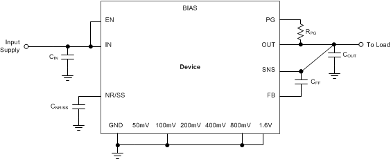 Figure 47. ANY-OUT Configuration Circuit
(3.3-V Output, No External Bias)
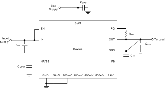 Figure 48. ANY-OUT Configuration Circuit
(0.9-V Output with Bias)
8.1.9 Increasing ANY-OUT Resolution for LILO Conditions
As with the adjustable operation, the output voltage is set according to Equation 5, except that R1 and R2 are internally integrated and matched for higher accuracy. Tying any of the ANY-OUT pins to SNS can increase the resolution of the internal feedback network by lowering the value of R1. One of the more useful pin combinations is to tie the 800mV pin to SNS, which reduces the resolution by 50% to 25 mV but limits the range. The new ANY-OUT ranges are 0.8 V to 1.175 V and 1.6 V to 1.975 V. The new additive output voltage levels are listed in Table 4.
Table 4. ANY-OUT Programmable Output Voltage with 800mV Tied to SNS
| ANY-OUT PROGRAM PINS (Active Low) | ADDITIVE OUTPUT VOLTAGE LEVEL |
|---|---|
| Pin 5 (50mV) | 25 mV |
| Pin 6 (100mV) | 50 mV |
| Pin 7 (200mV) | 100 mV |
| Pin 9 (400mV) | 200 mV |
| Pin 11 (1.6V) | 800 mV |
8.1.10 Current Sharing
Current sharing is possible through the use of external operational amplifiers. For more details, see the reference design 6A Current-Sharing Dual LDO, TIDU421.
8.1.11 Adjustable Operation
The TPS7A85 can either be used with the internal ANY-OUT network or by using external resistors. Using the ANY-OUT network allows the TPS7A85 to be programmed from 0.8 V to 3.95 V. To extend this output voltage range to 5.0 V, external resistors must be used. This configuration is referred to as the adjustable configuration of the TPS7A85 throughout this document. Regardless whether the internal resistor network or external resistors are used, the output voltage is set by two resistors, as shown in Figure 49. Using the internal resistor ensures a 1% accurate output voltage and minimizes the number of external components.
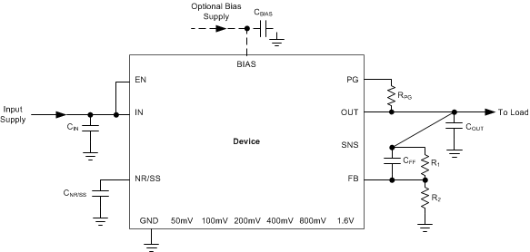 Figure 49. Adjustable Operation
R1 and R2 can be calculated for any output voltage range using Equation 8. This resistive network must provide a current equal to or greater than 5 μA for dc accuracy. Using an R1 of 12.1 kΩ is recommended to optimize the noise and PSRR.
Table 5 shows the resistor combinations required to achieve several common rails using standard 1%-tolerance resistors.
Table 5. Recommended Feedback-Resistor Values(1)
| TARGETED OUTPUT VOLTAGE (V) |
FEEDBACK RESISTOR VALUES | CALCULATED OUTPUT VOLTAGE (V) |
|
|---|---|---|---|
| R1 (kΩ) | R2 (kΩ) | ||
| 0.9 | 12.4 | 100 | 0.899 |
| 0.95 | 12.4 | 66.5 | 0.949 |
| 1.00 | 12.4 | 49.9 | 0.999 |
| 1.10 | 12.4 | 33.2 | 1.099 |
| 1.20 | 12.4 | 24.9 | 1.198 |
| 1.50 | 12.4 | 14.3 | 1.494 |
| 1.80 | 12.4 | 10 | 1.798 |
| 1.90 | 12.1 | 8.87 | 1.89 |
| 2.50 | 12.4 | 5.9 | 2.48 |
| 2.85 | 12.1 | 4.75 | 2.838 |
| 3.00 | 12.1 | 4.42 | 2.990 |
| 3.30 | 11.8 | 3.74 | 3.324 |
| 3.60 | 12.1 | 3.48 | 3.582 |
| 4.5 | 11.8 | 2.55 | 4.502 |
| 5.00 | 12.4 | 2.37 | 4.985 |
8.1.12 Sequencing Requirements
Supply and enable sequencing is only required when the bias rail is present. The start-up is always monotonic, independent of the sequencing requirements. Under these conditions the following requirements apply:
- VBIAS and VIN can be sequenced in any order, as long as VEN is tied to VIN or established after VIN, as shown in Figure 50.
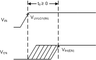 Figure 50. Sequencing Diagram
Two typical application circuits for implementing the sequencing requirements are detailed in the Sequencing with a Power-Good DC-DC Converter Pin and Sequencing with a Microcontroller (MCU) sections.
8.1.12.1 Sequencing with a Power-Good DC-DC Converter Pin
When a dc-dc converter is used to power the device and the PG of the dc-dc converter is used to enable the device, pull PG up to VIN, as shown in Figure 51.
 Figure 51. Sequencing with a DC-DC Converter and PG
8.1.12.2 Sequencing with a Microcontroller (MCU)
If a push-pull output stage is used to provide the enable signal to the device and the enable signal can possibly come before VIN when a bias is present (such as with an MCU), convert the enable signal to an open-drain signal as shown in Figure 52. Using an open-drain signal ensures that if the signal arrives before VIN, then the enable voltage does not violate the sequencing requirement.
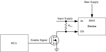 Figure 52. Push-Pull Enable to Open-Drain Enable
8.1.13 Power-Good (PG) Operation
To ensure proper operation of the power-good circuit, the pullup resistor value must be between 10 kΩ and 100 kΩ. The lower limit of 10 kΩ results from the maximum pulldown strength of the power-good transistor, and the upper limit of 100 kΩ results from the maximum leakage current at the power-good node. If the pullup resistor is outside of this range, then the power-good signal may not read a valid digital logic level.
Using a large CFF with a small CNR/SS causes the power-good signal to incorrectly indicate that the output voltage has settled during turn-on. The CFF time constant must be greater than the soft-start time constant to ensure proper operation of the PG during start-up. For a detailed description, see application report Pros and Cons of Using a Feed-Forward Capacitor with a Low Dropout Regulator, SBVA042.
The state of PG is only valid when the device operates above the minimum supply voltage. During short UVLO events and at light loads, power-good does not assert because the output voltage is sustained by the output capacitance.
8.1.14 Undervoltage Lockout (UVLO) Operation
The UVLO circuit ensures that the device stays disabled before its input or bias supplies reach the minimum operational voltage range, and ensures that the device shuts down when the input supply or bias supply collapse.
The UVLO circuit has a minimum response time of several microseconds to fully assert. During this time, a downward line transient below approximately 0.8 V causes the UVLO to assert for a short time; however, the UVLO circuit does not have enough stored energy to fully discharge the internal circuits inside of the device. When the UVLO circuit does not fully discharge, the internal circuits of the output are not fully disabled.
The effect of the downward line transient can be mitigated by either using a larger input capacitor to limit the fall time of the input supply when operating near the minimum VIN, or by using a bias rail.
Figure 53 shows the UVLO circuit response to various input voltage events. The diagram can be separated into the following parts:
- Region A: The device does not turn on until the input reaches the UVLO rising threshold.
- Region B: Normal operation with a regulated output
- Region C: Brownout event above the UVLO falling threshold (UVLO rising threshold – UVLO hysteresis). The output may fall out of regulation but the device is still enabled.
- Region D: Normal operation with a regulated output
- Region E: Brownout event below the UVLO falling threshold. The device is disabled in most cases and the output falls because of the load and active discharge circuit. The device is reenabled when the UVLO rising threshold is reached by the input voltage and a normal start-up then follows.
- Region F: Normal operation followed by the input falling to the UVLO falling threshold.
- Region G: The device is disabled when the input voltage falls below the UVLO falling threshold to 0 V. The output falls because of the load and active discharge circuit.
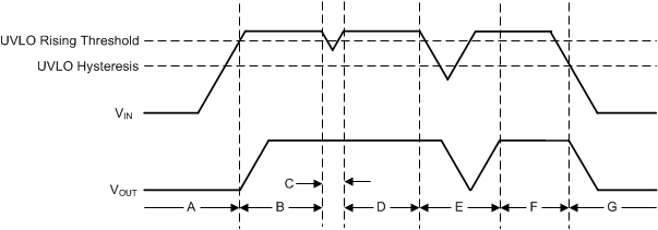 Figure 53. Typical UVLO Operation
8.1.15 Dropout Voltage (VDO)
Generally speaking, the dropout voltage often refers to the minimum voltage difference between the input and output voltage (VDO = VIN – VOUT) that is required for regulation. When VIN drops below the required VDO for the given load current, the device functions as a resistive switch and does not regulate output voltage. Dropout voltage is proportional to the output current because the device is operating as a resistive switch; see Figure 25, Figure 26, and Figure 27.
Dropout voltage is affected by the drive strength for the gate of the pass element, which is nonlinear with respect to VIN on this device because of the internal charge pump. The charge pump causes a higher dropout voltage at lower input voltages when a bias rail is not used, as illustrated in Figure 23.
For this device, dropout voltage increases exponentially when the input voltage nears its maximum operating voltage because the charge pump is internally clamped to 8.0 V; see Figure 23 and Figure 24.
8.1.16 Behavior when Transitioning from Dropout into Regulation
Some applications may have transients that place the device into dropout, especially because this device is a high-current linear regulator. A typical application with these conditions requires setting VIN ≤ VDO in order to keep the device junction temperature within its specified operating range. A load transient or line transient in these conditions can place the device into dropout, such as a load transient from 1 A to 4 A at 1A/µs when operating with a VIN of 5.4- V and a VOUT of 5.0 V.
The load transient saturates the error amplifier output stage when the pass element is fully driven on, thus making the pass element function like a resistor from VIN to VOUT. The error amplifier response time to this load transient (IOUT = 4 A to 1 A at 1 A/µs) is limited because the error amplifier must first recover from saturation and then place the pass element back into active mode. During the recovery from the load transient, VOUT overshoots because the pass element is functioning as a resistor from VIN to VOUT. If operating under these conditions, apply a higher dc load or increase the output capacitance to reduce the overshoot because these solutions provide a path to dissipate the excess charge.
8.1.17 Load Transient Response
The load-step transient response is the output voltage response by the LDO to a step in load current, whereby output voltage regulation is maintained; see Figure 18. There are two key transitions during a load transient response: the transition from a light to a heavy load and the transition from a heavy to a light load. The regions shown in Figure 54 are broken down in this section. Regions A, E, and H are where the output voltage is in steady-state.
During transitions from a light load to a heavy load, the:
- Initial voltage dip is a result of the depletion of the output capacitor charge and parasitic impedance to the output capacitor (region B).
- Recovery from the dip results from the LDO increasing its sourcing current, and leads to output voltage regulation (region C).
During transitions from a heavy load to a light load, the:
- Initial voltage rise results from the LDO sourcing a large current, and leads to the output capacitor charge to increase (region F).
- Recovery from the rise results from the LDO decreasing its sourcing current in combination with the load discharging the output capacitor (region G).
Transitions between current levels changes the internal power dissipation because the TPS7A85 is a high-current device (region D). The change in power dissipation changes the die temperature during these transitions, and leads to a slightly different voltage level. This different output voltage level shows up in the various load transient responses; see Figure 18.
A larger output capacitance reduces the peaks during a load transient but slows down the response time of the device. A larger dc load also reduces the peaks because the amplitude of the transition is lowered and a higher current discharge path is provided for the output capacitor; see Figure 20.
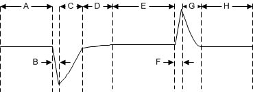 Figure 54. Load Transient Waveform
8.1.18 Negatively-Biased Output
The device does not start or operate as expected if the output voltage is pulled below ground. This issue commonly occurs when powering a split-rail system where the negative rail is established before the device is enabled. Several application solutions are possible, such as:
- Enable the device before the negative regulator and disable the device after the negative regulator.
- Delaying the EN voltage with respect to the IN voltage allows the internal pulldown resistor to discharge any voltage at OUT. If the discharge circuit is not strong enough to keep the output voltage at ground, then use an external pulldown resistor.
- Place a zener diode from IN to OUT to provide a small positive dc bias on the output when the input is supplied to the device, as shown in Figure 55.
- Use a PMOSFET to isolate the output of the device from the load causing the negative bias when the device is off, as shown in Figure 56.
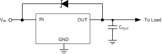 Figure 55. Zener Diode Placed from IN to OUT
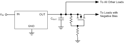 Figure 56. PMOSFET to Isolate the Output from the Load
8.1.19 Reverse Current Protection
As with most LDOs, this device can be damaged by excessive reverse current.
Conditions where excessive reverse current can occur are outlined in this section, all of which can exceed the absolute maximum rating of VOUT > VIN + 0.3 V:
- If the device has a large COUT, then the input supply collapses quickly and the load current becomes very small
- The output is biased when the input supply is not established
- The output is biased above the input supply
If an excessive reverse current flow is expected in the application, then external protection must be used to protect the device. Figure 57 shows one approach of protecting the device.
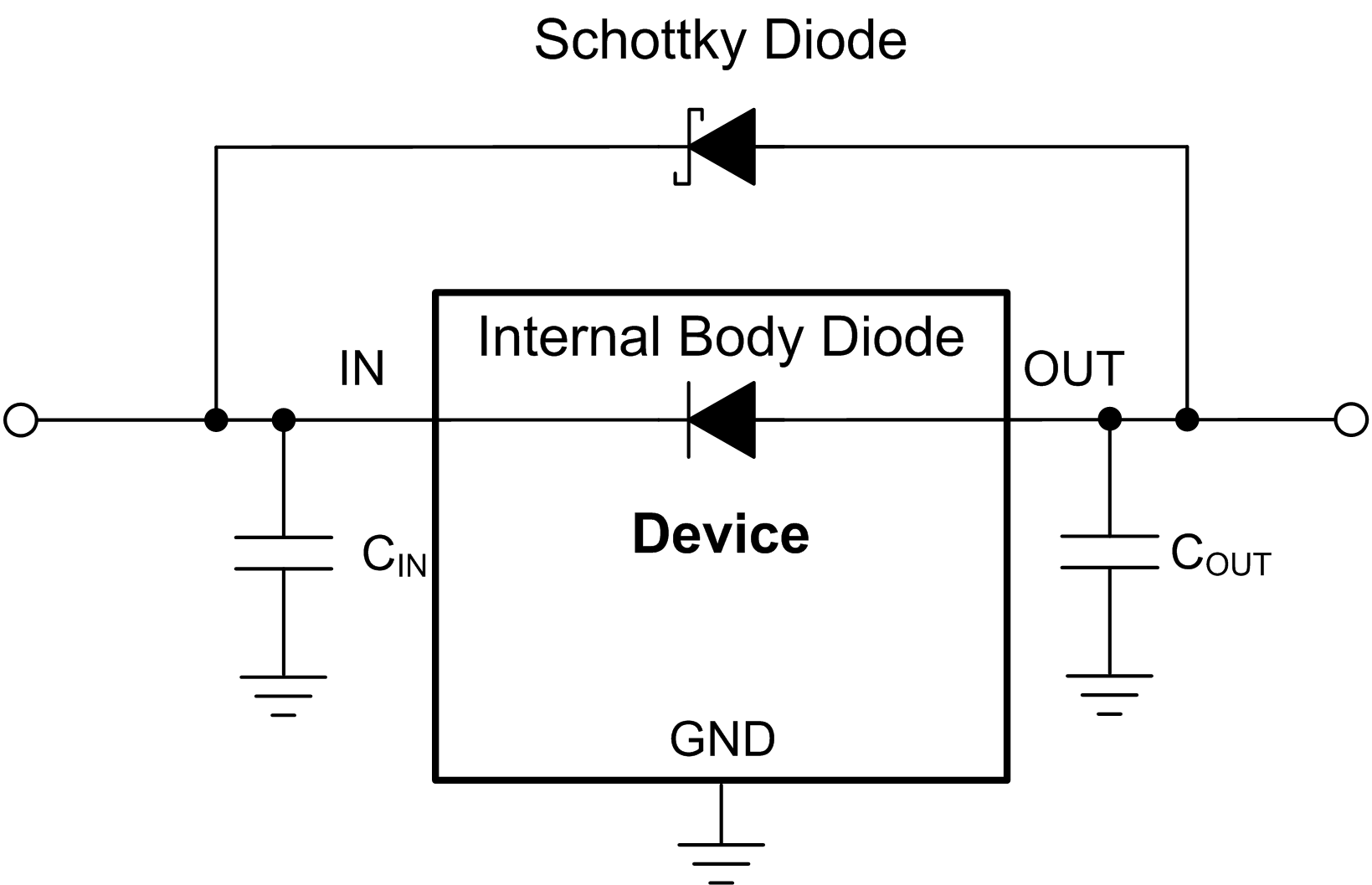 Figure 57. Example Circuit for Reverse Current Protection Using a Schottky Diode
8.1.20 Power Dissipation (PD)
Circuit reliability demands that proper consideration be given to device power dissipation, location of the circuit on the printed circuit board (PCB), and correct sizing of the thermal plane. The PCB area around the regulator must be as free as possible of other heat-generating devices that cause added thermal stresses.
As a first-order approximation, power dissipation in the regulator depends on the input-to-output voltage difference and load conditions. PD can be approximated using Equation 9:

An important note is that power dissipation can be minimized, and thus greater efficiency achieved, by proper selection of the system voltage rails. Proper selection allows the minimum input-to-output voltage differential to be obtained. The low dropout of the TPS7A85 allows for maximum efficiency across a wide range of output voltages.
The main heat conduction path for the device is through the thermal pad on the package. As such, the thermal pad must be soldered to a copper pad area under the device. This pad area contains an array of plated vias that conduct heat to any inner plane areas or to a bottom-side copper plane.
The maximum power dissipation determines the maximum allowable junction temperature (TJ) for the device. Power dissipation and junction temperature are most often related by the junction-to-ambient thermal resistance (θJA) of the combined PCB and device package and the temperature of the ambient air (TA), according to Equation 10. The equation is rearranged for output current in Equation 11.

Unfortunately, this thermal resistance (θJA) is highly dependent on the heat-spreading capability built into the particular PCB design, and therefore varies according to the total copper area, copper weight, and location of the planes. The θJA recorded in the Electrical Characteristics table is determined by the JEDEC standard, PCB, and copper-spreading area, and is only used as a relative measure of package thermal performance. Note that for a well-designed thermal layout, θJA is actually the sum of the VQFN package junction-to-case (bottom) thermal resistance (θJCbot) plus the thermal resistance contribution by the PCB copper.
8.1.20.1 Estimating Junction Temperature
The JEDEC standard now recommends the use of psi (Ψ) thermal metrics to estimate the junction temperatures of the LDO when in-circuit on a typical PCB board application. These metrics are not strictly speaking thermal resistances, but rather offer practical and relative means of estimating junction temperatures. These psi metrics are determined to be significantly independent of the copper-spreading area. The key thermal metrics (ΨJT and ΨJB) are given in the Electrical Characteristics table and are used in accordance with Equation 12.

where
- PD is the power dissipated as explained in Equation 9
- TT is the temperature at the center-top of the device package, and
- TB is the PCB surface temperature measured 1 mm from the device package and centered on the package edge
8.1.20.2 Recommended Area for Continuous Operation (RACO)
The operational area of an LDO is limited by the dropout voltage, output current, junction temperature, and input voltage. The recommended area for continuous operation for a linear regulator can be separated into the following parts, and is shown in Figure 58:
- Limited by dropout: Dropout voltage limits the minimum differential voltage between the input and the output (VIN – VOUT) at a given output current level; see the Dropout Voltage (VDO) section for more details.
- Limited by rated output current: The rated output current limits the maximum recommended output current level. Exceeding this rating causes the device to fall out of specification.
- Limited by thermals: The shape of the slope is given by Equation 11. The slope is nonlinear because the junction temperature of the LDO is controlled by the power dissipation across the LDO; therefore, when VIN – VOUT increases, the output current must decrease in order to ensure that the rated junction temperature of the device is not exceeded. Exceeding this rating can cause the device to fall out of specifications and reduces long-term reliability.
- Limited by VIN range: The rated input voltage range governs both the minimum and maximum of VIN – VOUT.
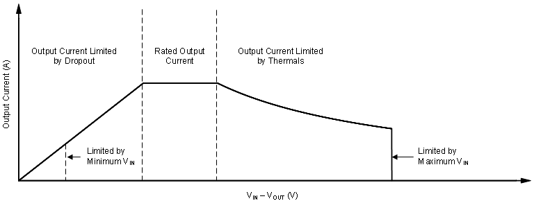 Figure 58. Continuous Operation Slope Region Description
Figure 59 to Figure 64 show the recommended area of operation curves for this device on a JEDEC-standard high-K board with a θJA = 35.4°C/W, as given in the Electrical Characteristics table.
 Figure 59. Recommended Area for Continuous Operation for VOUT = 0.9 V with Bias
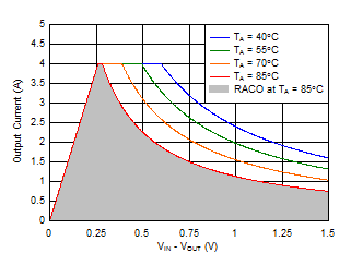 Figure 61. Recommended Area for Continuous Operation for VOUT = 1.8 V
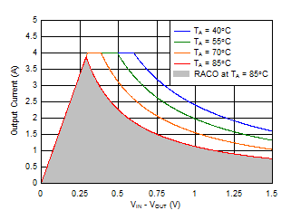 Figure 63. Recommended Area for Continuous Operation for VOUT = 3.3 V
 Figure 60. Recommended Area for Continuous Operation for VOUT = 1.2 V with Bias
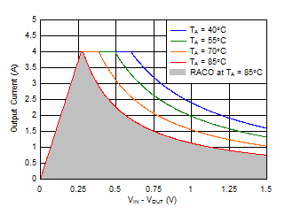 Figure 62. Recommended Area for Continuous Operation for VOUT = 2.5 V
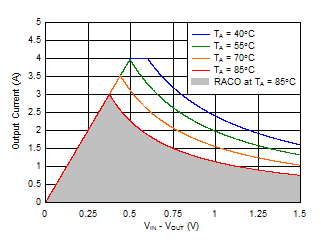 Figure 64. Recommended Area for Continuous Operation for VOUT = 5.0 V
8.2 Typical Applications
8.2.1 Low-Input, Low-Output (LILO) Voltage Conditions
This section discusses the implementation of the TPS7A85 using the ANY-OUT configuration to regulate a 4.0-A load requiring good PSRR at high frequency with low noise at 0.9 V using a 1.3-V input voltage and a 5.0-V bias supply. The schematic for this typical application circuit is provided in Figure 65.
 Figure 65. Typical Application
8.2.1.1 Design Requirements
For this design example, use the parameters listed in Table 6 as the input parameters.
Table 6. Design Parameters
| PARAMETER | DESIGN REQUIREMENT |
|---|---|
| Input voltage | 1.4 V, ±3%, provided by the dc-dc converter switching at 500 kHz |
| Output voltage | 0.9 V, ±1% |
| Output current | 4.0 A (maximum), 100 mA (minimum) |
| RMS noise, 10 Hz to 100 kHz | < 10 µVRMS |
| PSRR at 500 kHz | > 40 dB |
| Start-up time | < 25 ms |
8.2.1.2 Detailed Design Procedure
For these conditions, the maximum dropout of the TPS7A85 is approximately 240 mV, thus a 400-mV headroom is sufficient for operation over both input and output voltage accuracy. The bias rail is provided for better performance for the LILO conditions. PSRR is greater than 40 dB in these conditions, as per Figure 2. Noise is less than 10 µVRMS, as per Figure 11.
The ANY-OUT internal resistor network is also used for maximum accuracy.
To achieve 0.9 V on the output, the 100mV pin is grounded. The voltage value of 100 mV is added to the 0.8-V internal reference voltage for VOUT(nom) equal to 0.9 V, as described in Equation 13.
Input and output capacitors are selected in accordance with the Recommended Capacitor Types section. Ceramic capacitances of 47 µF for the input and one 47-µF capacitor in parallel with two 10-µF capacitors for the output are selected.
To satisfy the required start-up time and still maintain low-noise performance, a 100-nF CNR/SS is selected. This value is calculated with Equation 14. To further minimize noise, a feed-forward capacitance (CFF) of 10 nF is selected.
The maximum ambient temperature for this application is 40°C based on Figure 59 and given the 3% accuracy of the input supply.
8.2.1.3 Application Curves
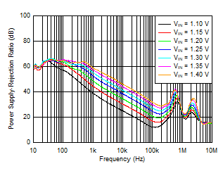 Figure 66. Output PSRR
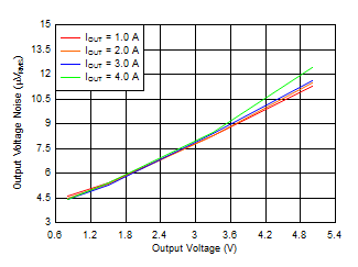 Figure 67. Output Noise Level
8.2.2 Typical Application for a 5.0-V Rail
This section discusses the implementation of the TPS7A85 using an adjustable feedback network to regulate a 4-A load requiring good PSRR at high frequency with low noise at an output voltage of 5.0 V. The schematic for this typical application circuit is provided in Figure 68.
 Figure 68. Typical Application
8.2.2.1 Design Requirements
For this design example, use the parameters listed in Table 6 as the input parameters.
Table 7. Design Parameters
| PARAMETER | DESIGN REQUIREMENT |
|---|---|
| Input voltage | 5.60 V, ±1%, provided by the dc-dc converter switching at 500 kHz |
| Output voltage | 5.0 V, ±1% |
| Output current | 4.0 A (maximum), 10 mA (minimum) |
| Start-up time | < 25 ms |
8.2.2.2 Detailed Design Procedure
For these conditions, the maximum dropout of the TPS7A85 is approximately 500 mV, thus a 600-mV headroom is sufficient for operation over both input and output voltage accuracy. At full load and high temperature on some devices, the TPS7A85 can enter dropout if both the input and output supply are beyond the edges of their accuracy specification.
For a 5.0-V output, use external adjustable resistors. See the resistor values in listed Table 5 for choosing resistors for a 5.0-V output.
Input and output capacitors are selected in accordance with the Recommended Capacitor Types section. Ceramic capacitances of 47 µF for the input and one 47-µF capacitor in parallel with two 10-µF capacitors for the output are selected. To further minimize noise, a feed-forward capacitance (CFF) of 10 nF is selected.
To satisfy the required start-up time and still maintain low-noise performance, a 100-nF CNR/SS is selected. This value is calculated with Equation 14.
The maximum ambient temperature for this application is 40°C based on Figure 64 and given the 1% accuracy of the input supply. This temperature can still exceed the maximum junction temperature, but the 4.0-A load is a short pulse requirement and not a dc load so the thermal effects are minimal.
8.2.2.3 Application Curves
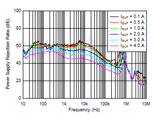 Figure 69. PSRR vs Frequency and IOUT for VOUT = 5.0 V with VIN = 5.6 V
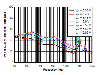 Figure 70. PSRR vs Frequency and VIN for VOUT = 5.0 V at IOUT = 4.0 A