ZHCSEI2B January 2016 – June 2021 TPS7A84
PRODUCTION DATA
- 1 特性
- 2 应用
- 3 说明
- 4 Revision History
- 5 Pin Configurations and Functions
- 6 Specifications
- 7 Detailed Description
-
8 Application and Implementation
- 8.1
Application Information
- 8.1.1 Recommended Capacitor Types
- 8.1.2 Input and Output Capacitor Requirements (CIN and COUT)
- 8.1.3 Noise-Reduction and Soft-Start Capacitor (CNR/SS)
- 8.1.4 Feed-Forward Capacitor (CFF)
- 8.1.5 Soft-Start and In-Rush Current
- 8.1.6 Optimizing Noise and PSRR
- 8.1.7 Charge Pump Noise
- 8.1.8 ANY-OUT Programmable Output Voltage
- 8.1.9 ANY-OUT Operation
- 8.1.10 Increasing ANY-OUT Resolution for LILO Conditions
- 8.1.11 Current Sharing
- 8.1.12 Adjustable Operation
- 8.1.13 Sequencing Requirements
- 8.1.14 Power-Good Operation
- 8.1.15 Undervoltage Lockout (UVLO) Operation
- 8.1.16 Dropout Voltage (VDO)
- 8.1.17 Behavior when Transitioning from Dropout into Regulation
- 8.1.18 Load Transient Response
- 8.1.19 Negatively-Biased Output
- 8.1.20 Reverse Current Protection
- 8.1.21 Power Dissipation (PD)
- 8.1.22 Estimating Junction Temperature
- 8.1.23 Recommended Area for Continuous Operation (RACO)
- 8.2 Typical Applications
- 8.1
Application Information
- 9 Power Supply Recommendations
- 10Layout
- 11Device and Documentation Support
- 12Mechanical, Packaging, and Orderable Information
8.1.5 Soft-Start and In-Rush Current
Soft-start refers to the ramp-up characteristic of the output voltage during LDO turn-on after EN and UVLO achieve threshold voltage. The noise-reduction capacitor serves a dual purpose of both governing output noise reduction and programming the soft-start ramp during turn-on.
In-rush current is defined as the current into the LDO at the IN pin during start-up. In-rush current then consists primarily of the sum of load current and the current used to charge the output capacitor. This current is difficult to measure because the input capacitor must be removed, which is not recommended. However, this soft-start current can be estimated by Equation 3:
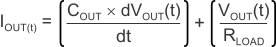
where:
- VOUT(t) is the instantaneous output voltage of the turn-on ramp
- dVOUT(t) / dt is the slope of the VOUT ramp
- RLOAD is the resistive load impedance