ZHCSBA4E May 2013 – August 2014 TPS7A8300
PRODUCTION DATA.
- 1 特性
- 2 应用范围
- 3 说明
- 4 修订历史记录
- 5 Pin Configurations and Functions
- 6 Specifications
-
7 Detailed Description
- 7.1 Overview
- 7.2 Functional Block Diagram
- 7.3
Feature Description
- 7.3.1 ANY-OUT Programmable Output Voltage
- 7.3.2 Adjustable Operation
- 7.3.3 ANY-OUT Operation
- 7.3.4 2-A LDO with an Internal Charge Pump
- 7.3.5 Low-Noise, 0.8-V Reference
- 7.3.6 Internal Protection Circuitry
- 7.3.7 Programmable Soft-Start
- 7.3.8 Power-Good Function
- 7.3.9 Integrated Resistance Network (ANY-OUT)
- 7.4 Device Functional Modes
- 8 Application and Implementation
- 9 Power-Supply Recommendations
- 10Layout
- 11器件和文档支持
- 12机械封装和可订购信息
封装选项
机械数据 (封装 | 引脚)
散热焊盘机械数据 (封装 | 引脚)
订购信息
5 Pin Configurations and Functions
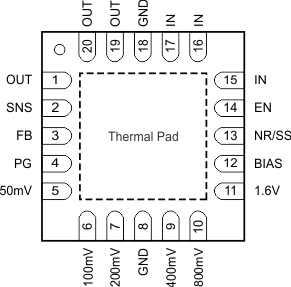
Pin Functions
| PIN | DESCRIPTION | ||
|---|---|---|---|
| NAME | NO. | I/O | |
| 50mV, 100mV, 200mV, 400mV, 800mV, 1.6V | 5, 6, 7, 9, 10, 11 | I | Output voltage setting pins. These pins should be connected to ground or left floating. Connecting these pins to ground increases the output voltage by the value of the pin name; multiple pins can be simultaneously connected to GND to select the desired output voltage. Leave these pins floating (open) when not in use. See the ANY-OUT Programmable Output Voltage section for more details. |
| BIAS | 12 | I | BIAS supply voltage pin for the use of 1.1 V ≤ VIN ≤ 1.4 V and to connect a 10-µF capacitor between this pin and ground. |
| EN | 14 | I | Enable pin. Driving this pin to logic high enables the device; driving this pin to logic low disables the device. See the Start-Up section for more details. |
| FB | 3 | I | Output voltage feedback pin connected to the error amplifier. Although not required, a 10-nF feed-forward capacitor from FB to OUT (as close to the device as possible) is recommended for low-noise applications to maximize ac performance. The use of a feed-forward capacitor may disrupt PG (power good) functionality. See the ANY-OUT Programmable Output Voltage and Adjustable Operation sections for more details. |
| GND | 8, 18 | — | Ground pin. These pins must be externally shorted for the RGR package option. |
| IN | 15-17 | I | Input supply voltage pin. A 10-μF input ceramic capacitor is required. See the Input and Output Capacitor Requirements (CIN and COUT) section for more details. |
| OUT | 1, 19, 20 | O | Regulated output pin. A 22-μF or larger ceramic capacitor is required for stability (a 10-μF minimum effective capacitance is required). See the Input and Output Capacitor Requirements (CIN and COUT) section for more details. |
| PG | 4 | O | Active-high power-good pin. An open-drain output indicates when the output voltage reaches 89% of the target. The use of a feed-forward capacitor may disrupt PG (power good) functionality. See the Power-Good Function section for more details. |
| SNS | 2 | I | Output voltage sense input pin. Connect this pin only if the ANY-OUT feature is used. See the ANY-OUT Programmable Output Voltage and Adjustable Operation sections for more details. |
| NR/SS | 13 | — | Noise-reduction and soft-start pin. Connecting an external capacitor between this pin and ground reduces reference voltage noise and also enables the soft-start function. Although not required, a capacitor is recommended for low-noise applications to connect a 10-nF capacitor from NR/SS to GND (as close to the device as possible) to maximize ac performance. See the Noise-Reduction and Soft-Start Capacitor (CNR/SS) section for more details. |
| Thermal Pad | Pad | — | Connect the thermal pad to a large-area ground plane. The thermal pad is internally connected to GND. |