ZHCSBA4E May 2013 – August 2014 TPS7A8300
PRODUCTION DATA.
- 1 特性
- 2 应用范围
- 3 说明
- 4 修订历史记录
- 5 Pin Configurations and Functions
- 6 Specifications
-
7 Detailed Description
- 7.1 Overview
- 7.2 Functional Block Diagram
- 7.3
Feature Description
- 7.3.1 ANY-OUT Programmable Output Voltage
- 7.3.2 Adjustable Operation
- 7.3.3 ANY-OUT Operation
- 7.3.4 2-A LDO with an Internal Charge Pump
- 7.3.5 Low-Noise, 0.8-V Reference
- 7.3.6 Internal Protection Circuitry
- 7.3.7 Programmable Soft-Start
- 7.3.8 Power-Good Function
- 7.3.9 Integrated Resistance Network (ANY-OUT)
- 7.4 Device Functional Modes
- 8 Application and Implementation
- 9 Power-Supply Recommendations
- 10Layout
- 11器件和文档支持
- 12机械封装和可订购信息
封装选项
机械数据 (封装 | 引脚)
散热焊盘机械数据 (封装 | 引脚)
订购信息
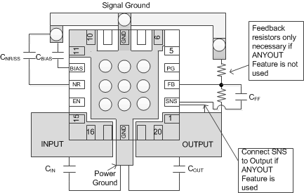
10 Layout
10.1 Layout Guidelines
10.1.1 Board Layout
For best overall performance, place all circuit components on the same side of the circuit board and as near as practical to the respective LDO pin connections. Place ground return connections to the input and output capacitor, and to the LDO ground pin as close to each other as possible, connected by a wide, component-side, copper surface. The use of vias and long traces to create LDO circuit connections is strongly discouraged and negatively affects system performance. This grounding and layout scheme minimizes inductive parasitics, and thereby reduces load-current transients, minimizes noise, and increases circuit stability.
A ground reference plane is also recommended and is either embedded in the PCB itself or located on the bottom side of the PCB opposite the components. This reference plane serves to assure accuracy of the output voltage, shield noise, and behaves similar to a thermal plane to spread (or sink) heat from the LDO device when connected to the PowerPAD™. In most applications, this ground plane is necessary to meet thermal requirements.