ZHCSO39B May 2022 – August 2022 TPS7A74
PRODUCTION DATA
- 1 特性
- 2 应用
- 3 说明
- 4 Revision History
- 5 Pin Configuration and Functions
- 6 Specifications
- 7 Detailed Description
- 8 Application and Implementation
- 9 Device and Documentation Support
- 10Mechanical, Packaging, and Orderable Information
8.4.1 Layout Guidelines
An optimal layout can greatly improve transient performance, PSRR, and noise. To minimize the voltage drop on the input of the device during load transients, the capacitance on IN and BIAS must be connected as close as possible to the device. This capacitance also minimizes the effects of parasitic inductance and resistance of the input source and can, therefore, improve stability. To achieve optimal transient performance and accuracy, the top side of R1 in Figure 8-1 must be connected as close as possible to the load. If BIAS is connected to IN, connect BIAS as close to the sense point of the input supply as possible. This connection minimizes the voltage drop on BIAS during transient conditions and can improve the turn-on response.
Knowing the device power dissipation and proper sizing of the thermal plane that is connected to the thermal pad is critical to avoiding thermal shutdown and ensuring reliable operation. Power dissipation (PD) of the device depends on input voltage and load conditions. Equation 9 calculates PD.

Power dissipation can be minimized and greater efficiency can be achieved by using the lowest possible input voltage necessary to achieve the required output voltage regulation.
On the WSON (DSD) package, the primary conduction path for heat is through the exposed pad to the printed circuit board (PCB). The pad can be connected to ground or left floating; however, this pad must be attached to an appropriate amount of copper PCB area to ensure the device does not overheat. The maximum junction-to-ambient thermal resistance depends on the maximum ambient temperature, maximum device junction temperature, and power dissipation of the device. Equation 10 calculates the maximum junction-to-ambient thermal resistance.
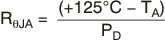
When the device is mounted on an application PCB, TI strongly recommends using ΨJT and Ψ