ZHCSER8 December 2015 TPS7A6650H-Q1
PRODUCTION DATA.
7 Detailed Description
7.1 Overview
This product is a combination of a low-dropout linear regulator with reset function. The power-on reset initializes once the Vout output exceeds 91.6% of the target value. The power-on-reset delay is a function of the value set by an external capacitor on the CT pin before releasing the PG pin high.
7.2 Functional Block Diagram
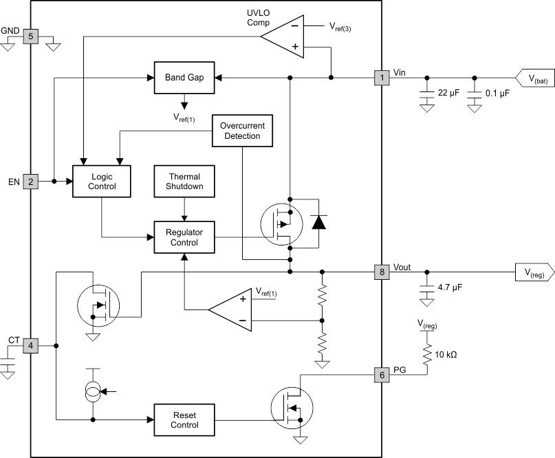
 Figure 13. TPS7A6650H-Q1 Functional Block Diagram
7.3 Feature Description
7.3.1 Enable (EN)
This is a high-voltage-tolerant pin; high input activates the device and turns the regulator ON. One can connect this input to the Vin pin for self-bias applications.
7.3.2 Regulated Output (Vout)
This is the regulated output based on the required voltage. The output has current limitation. During initial power up, the regulator has a soft start incorporated to control initial current through the pass element and the output capacitor.
In the event the regulator drops out of regulation, the output tracks the input minus a drop based on the load current. When the input voltage drops below the UVLO threshold, the regulator shuts down until the input voltage recovers above the minimum start-up level.
7.3.3 Power-On Reset (PG)
This is an output with an external pullup resistor to the regulated supply. The output remains low until the regulated Vout has exceeded approximately 90% of the set value and the power-on-reset delay has expired. The on-chip oscillator presets the delay. The regulated output falling below the 90% level asserts this output low after a short de-glitch time of approximately 250 µs (typical).
7.3.4 Reset Delay Timer (CT)
An external capacitor on this pin sets the timer delay before the reset pin is asserted high. The constant output current charges an external capacitor until the voltage exceeds a threshold to trip an internal comparator. If this pin is open, the default delay time is 290 µs (typ). After releasing the PG pin high, the capacitor on this pin discharges, thus allowing the capacitor to charge from approximately 0.2 V for the next power-on-reset delay-timer function.
An external capacitor, CT, defines the reset-pulse delay time, t(POR), with the charge time of:

The power-on reset initializes once the output V(Vout) exceeds 91.6% of the programmed value. The power-on-reset delay is a function of the value set by an external capacitor on the CT pin before the releasing of the PG pin high.
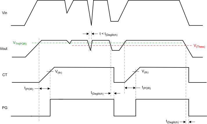
 Figure 14. Conditions for Activation of Reset
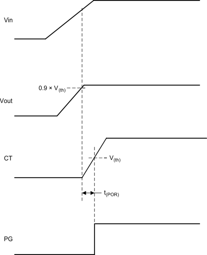
 Figure 15. External Programmable Reset Delay
7.3.5 Undervoltage Shutdown
There is an internally fixed undervoltage shutdown threshold. Undervoltage shutdown activates when the input voltage on Vin drops below V(VinUVLO). This ensures the regulator is not latched into an unknown state during low input supply voltage. If the input voltage has a negative transient which drops below the UVLO threshold and recovers, the regulator shuts down and powers up with a normal power-up sequence once the input voltage is above the required levels.
7.3.6 Low-Voltage Tracking
At low input voltages, the regulator drops out of regulation and the output voltage tracks input minus a voltage based on the load current (IO) and switch resistance (R(SW)). This allows for a smaller input capacitor and can possibly eliminate the need of using a boost convertor during cold-crank conditions.
7.3.7 Thermal Shutdown
These devices incorporate a thermal shutdown (TSD) circuit as a protection from overheating. For continuous normal operation, the junction temperature should not exceed the TSD trip point. If the junction temperature exceeds the TSD trip point, the output turns off. When the junction temperature falls below the TSD trip point, the output turns on again.
Thermal protection disables the output when the junction temperature rises to approximately 175°C, allowing the device to cool. Cooling of the junction temperature to approximately 155°C enables the output circuitry. Depending on power dissipation, thermal resistance, and ambient temperature, the thermal protection circuit may cycle on and off. This cycling limits the dissipation of the regulator, protecting it from damage as a result of overheating.
The purpose of the design of the internal protection circuitry of the TPS7A6650H-Q1 is for protection against overload conditions, not as a replacement for proper heat-sinking. Continuously running the TPS7A6650H-Q1 device into thermal shutdown degrades device reliability.
7.4 Device Functional Modes
7.4.1 Operation With V(VIN) < 4 V
The devices operate with input voltages above 4 V. The maximum UVLO voltage is 2.6 V, and the devices operate at an input voltage above 4 V. The devices can also operate at lower input voltages; no minimum UVLO voltage is specified. At input voltages below the actual UVLO voltage, the devices do not operate.
7.4.2 Operation With EN Control
The enable rising edge threshold voltage is 1.7 V (maximum). With the EN pin held above that voltage and the input voltage above 4 V, the device becomes active. The enable falling edge is 0.4 V (minimum). Holding the EN pin below that voltage disables the device, thus reducing the IC quiescent current.