SBVS163A June 2011 – May 2015 TPS7A3401
PRODUCTION DATA.
- 1 Features
- 2 Applications
- 3 Description
- 4 Revision History
- 5 Pin Configuration and Functions
- 6 Specifications
- 7 Detailed Description
- 8 Application and Implementation
- 9 Power Supply Recommendations
- 10Layout
- 11Device and Documentation Support
- 12Mechanical, Packaging, and Orderable Information
8 Application and Implementation
NOTE
Information in the following applications sections is not part of the TI component specification, and TI does not warrant its accuracy or completeness. TI’s customers are responsible for determining suitability of components for their purposes. Customers should validate and test their design implementation to confirm system functionality.
8.1 Application Information
The TPS7A3401 device belongs to a family of new generation linear regulators that use an innovative bipolar process to achieve ultralow-noise. As a bipolar-based device, the TPS7A3401 device is ideal for high-accuracy, high-performance analog applications at higher voltages.
8.1.1 Adjustable Operation
The TPS7A3401 device has an output voltage range from –1.174 V to –18 V. The nominal output voltage of the device is set by two external resistors, as shown in Figure 19.
 Figure 19. Adjustable Operation for Maximum AC Performance
R1 and R2 can be calculated for any output voltage range using the formula shown in Equation 1. To ensure stability under no load conditions, this resistive network must provide a current equal to or greater than 5 μA.

If greater voltage accuracy is required, consider the output voltage offset contributions because of the feedback pin current and use 0.1% tolerance resistors.
8.1.2 Transient Response
As with any regulator, increasing the size of the output capacitor reduces overshoot and undershoot magnitude but increases duration of the transient response.
8.1.3 Post DC-DC Converter Filtering
Most of the time, the voltage rails available in a system do not match the voltage specifications demanded by one or more of its circuits; these rails must be stepped up or down, depending on specific voltage requirements.
DC-DC converters are the preferred solution to step up or down a voltage rail when current consumption is not negligible. They offer high-efficiency with minimum heat generation, but they have one primary disadvantage: they introduce a high-frequency component, and the associated harmonics, on top of the DC output signal.
This high-frequency component, if not filtered properly, degrades analog circuitry performance, reducing overall system accuracy and precision.
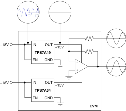
The TPS7A3401 device offers a wide-bandwidth, very high power-supply rejection ratio. This specification makes it ideal for post DC-DC converter filtering, as shown in Figure 20. TI highly recommends using the maximum performance schematic shown in Figure 19. Also, verify that the fundamental frequency (and its first harmonic, if possible) is within the bandwidth of the regulator PSRR, shown in Figure 15.
 Figure 20. Post DC-DC Converter Regulation to High-Performance Analog Circuitry
8.1.4 Power for Precision Analog
One of the primary applications of the TPS7A3401 device is to provide ultralow-noise voltage rails to high-performance analog circuitry to maximize system accuracy and precision.
The TPS7A3401 negative high-voltage linear regulator provides ultralow noise positive and negative voltage rails to high-performance analog circuitry, such as operational amplifiers, ADCs, DACs, and audio amplifiers.
Because of the ultralow noise levels at high voltages, analog circuitry with high-voltage input supplies can be used. This characteristic allows for high-performance analog solutions to optimize the voltage range, maximizing system accuracy.
8.2 Typical Application
 Figure 21. Maximize PSRR Performance and Minimize RMS Noise
8.2.1 Design Requirements
The design goals are VIN = –3 V, VOUT = –1.2 V, and IOUT = 150 mA, maximum. The input supply comes from a supply on the same printed-circuit-board (PCB). The design circuit is shown in Figure 19.
The design space consists of CIN, COUT, CFF, R1, and R2, at TA(max) = 75°C.
8.2.2 Detailed Design Procedure
The first step when designing with a linear regulator is to examine the maximum load current along with the input and output voltage requirements to determine if the device thermal and dropout voltage requirements can be met. At 150 mA, the input dropout voltage of the TPS7A3401 family is a maximum of 800 mV over temperature; therefore, the dropout headroom of 1.8 V is sufficient for operation over both input and output voltage accuracy. Dropout headroom is calculated as VIN – VOUT – VDO(max), and should be greater than 0 for reliable operation. VDO(max) is the maximum dropout allowed, given worst-case load conditions.
The maximum power dissipated in the linear regulator is the maximum voltage dropped across the pass element from the input to the output, multiplied by the maximum load current. In this example, the maximum voltage drop across in the pass element is |3 V – 1.2 V|, giving us a VDO = 1.8 V. The power dissipated in the pass element is calculated by taking this voltage drop multiplied by the maximum load current. For this example, the maximum power dissipated in the linear regulator is 0.273 W, and is calculated using Equation 2.
Once the power dissipated in the linear regulator is known, the corresponding junction temperature rise can be calculated. To calculate the junction temperature rise above ambient, the power dissipated must be multiplied by the junction-to-ambient thermal resistance. This calculation gives the worst-case junction temperature; good thermal design can significantly reduce this number. For thermal resistance information, refer to Thermal Information. For this example, using the DGN package, the maximum junction temperature rise is calculated to be 17.3°C. The maximum junction temperature rise is calculated by adding junction temperature rise to the maximum ambient temperature, which is 75°C for this example. For this example, the designer calculates the maximum junction temperature is 92.3°C. Keep in mind the maximum junction temperate must be less than 125°C for reliable device operation. Additional ground planes, added thermal vias, and air flow all help to lower the maximum junction temperature.
Use the following equations to pick the rest of the components:
To ensure stability under no-load conditions, the current through the resistor network must be greater than 5 µA, as shown in Equation 3.

To set R2 = 100 kΩ for a standard 1% value resistor, we calculate R1 as shown in Equation 4.

Use a standard, 1%, 2.05-kΩ resistor for R1.
For CIN, assume that the –3-V supply has some inductance, and is placed several inches away from the PCB. For this case, we select a 2.2-µF ceramic input capacitor to ensure that the input impedance is negligible to the LDO control loop while keep the physical size and cost of the capacitor low; this component is a common-value capacitor.
For better PSRR for this design, use a 10-µF input and output capacitor. To reduce the peaks from transients but slow down the recovery time, increase the output capacitor size or add additional output capacitors.
8.2.2.1 Capacitor Recommendations
Low-ESR capacitors should be used for the input, output, noise reduction, and feed-forward capacitors. Ceramic capacitors with X7R and X5R dielectrics are preferred. These dielectrics offer more stable characteristics. Ceramic X7R capacitors offer improved overtemperature performance, while ceramic X5R capacitors are the most cost-effective and are available in higher values.
High-ESR capacitors may degrade PSRR.
8.2.2.1.1 Input and Output Capacitor Requirements
The TPS7A3401 negative, high-voltage linear regulator achieves stability with a minimum input and output capacitance of 2.2 μF; however, TI highly recommends using a 10-μF capacitor to maximize AC performance.
8.2.2.1.2 Feed-Forward Capacitor Requirements
Although feed-forward capacitors (CFF) are not needed to achieve stability, TI highly recommends using 10-nF capacitors to minimize noise and maximize AC performance.
For more information on CFF, refer to Application Report, Pros and Cons of Using a Feedforward Capacitor with a Low-Dropout Regulator (SBVA042). This application report explains the advantages of using CFF (also known as CBYP), and the problems that can occur while using this capacitor.
8.2.3 Application Curves


8.3 Do's and Don'ts
Place at least one, low-ESR, 2.2-μF capacitor as close as possible to both the IN and OUT terminals of the regulator to the GND pin.
Provide adequate thermal paths away from the device.
Do not place the input or output capacitor more than 10 mm away from the regulator.
Do not exceed the absolute maximum ratings.
Do not float the Enable (EN) pin.