ZHCSOY3L January   2005  – February 2022 TPS799

PRODUCTION DATA  

  1. 特性
  2. 应用
  3. 描述
  4. Revision History
  5. Pin Configuration and Functions
  6. Specifications
    1. 6.1 Absolute Maximum Ratings
    2. 6.2 ESD Ratings
    3. 6.3 Recommended Operating Conditions
    4. 6.4 Thermal Information
    5. 6.5 Electrical Characteristics
    6. 6.6 Typical Characteristics
  7. Detailed Description
    1. 7.1 Overview
    2. 7.2 Functional Block Diagrams
    3. 7.3 Feature Description
      1. 7.3.1 Internal Current Limit
      2. 7.3.2 Shutdown
      3. 7.3.3 Start Up
      4. 7.3.4 Undervoltage Lockout (UVLO)
    4. 7.4 Device Functional Modes
  8. Application and Implementation
    1. 8.1 Application Information
    2. 8.2 Typical Application
      1. 8.2.1 Design Requirements
      2. 8.2.2 Detailed Design Procedure
        1. 8.2.2.1 Input and Output Capacitor Requirements
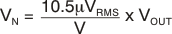
        2. 8.2.2.2 Output Noise
        3. 8.2.2.3 Dropout Voltage
        4. 8.2.2.4 Transient Response
        5. 8.2.2.5 Minimum Load
        6. 8.2.2.6 Feedback Capacitor Requirements (TPS79901 Only)
      3. 8.2.3 Application Curve
    3. 8.3 What To Do and What Not To Do
  9. Power Supply Recommendations
  10. 10Layout
    1. 10.1 Layout Guidelines
      1. 10.1.1 Board Layout Recommendations to Improve PSRR and Noise Performance
      2. 10.1.2 Thermal Information
        1. 10.1.2.1 Thermal Protection
        2. 10.1.2.2 Power Dissipation
        3. 10.1.2.3 Package Mounting
    2. 10.2 Layout Example
  11. 11Device and Documentation Support
    1. 11.1 Device Support
      1. 11.1.1 Development Support
        1. 11.1.1.1 Evaluation Modules
        2. 11.1.1.2 Spice Models
      2. 11.1.2 Device Nomenclature
    2. 11.2 Documentation Support
      1. 11.2.1 Related Documentation
    3. 11.3 接收文档更新通知
    4. 11.4 支持资源
    5. 11.5 Trademarks
    6. 11.6 Electrostatic Discharge Caution
    7. 11.7 术语表
  12. 12Mechanical, Packaging, and Orderable Information

封装选项

机械数据 (封装 | 引脚)
散热焊盘机械数据 (封装 | 引脚)
订购信息

Output Noise

In most LDOs, the band gap is the dominant noise source. If a noise-reduction capacitor (CNR) is used with the TPS799, the band gap does not contribute significantly to noise. Instead, noise is dominated by the output resistor divider and the error amplifier input. To minimize noise in a given application, use a 0.01-μF noise reduction capacitor. To further optimize noise, equivalent series resistance of the output capacitor can be set to approximately 0.2 Ω. This configuration maximizes phase margin in the control loop, reducing total output noise by up to 10%.

Noise can be referred to the feedback point; with CNR = 0.01 μF total noise is approximately given by Equation 1:

Equation 1. GUID-04B885CC-097F-48FA-86F0-3DF5FF9A85B5-low.gif