SBVS133A February 2010 – November 2014 TPS783
PRODUCTION DATA.
- 1 Features
- 2 Applications
- 3 Description
- 4 Revision History
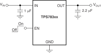
- 5 Pin Configuration and Functions
- 6 Specifications
- 7 Detailed Description
- 8 Application and Implementation
- 9 Power-Supply Recommendations
- 10Layout
- 11Device and Documentation Support
- 12Mechanical, Packaging, and Orderable Information
8 Application and Implementation
NOTE
Information in the following applications sections is not part of the TI component specification, and TI does not warrant its accuracy or completeness. TI’s customers are responsible for determining suitability of components for their purposes. Customers should validate and test their design implementation to confirm system functionality.
8.1 Application Information
The TPS783 family of LDOs is factory-programmable to have a fixed output. Note that during startup or steady-state conditions, do not allow the EN pin voltage to exceed VIN + 0.3 V.
8.2 Typical Application
8.2.1 Design Requirements
8.2.1.1 Input and Output Capacitor Requirements
A 0.1-μF input capacitor is necessary for stable operation. Good analog design practice is to connect a 0.1-μF to 1.0-μF, low equivalent series resistance (ESR) capacitor across the input supply near the regulator. This capacitor counteracts reactive input sources and improves transient response, noise rejection, and ripple rejection. A higher-value capacitor may be necessary if large, fast rise-time load transients are anticipated, or if the device is not located near the power source.
The TPS783 family is designed to be stable with standard ceramic capacitors with values of 1.0 μF or larger at the output. X5R- and X7R-type capacitors are best because they have minimal variation in value and ESR over temperature. Maximum ESR must be less than 1.0 Ω. With tolerance and dc bias effects, the minimum capacitance for stable operation is 1 μF.
8.2.1.2 Dropout Voltage
The TPS783 family uses a PMOS pass transistor to achieve low dropout. When (VIN – VOUT) is less than the dropout voltage (VDO), the PMOS pass device is the linear region of operation and the input-to-output resistance is the RDS(ON) of the PMOS pass element. VDO approximately scales with output current because the PMOS device behaves like a resistor in dropout. As with any linear regulator, PSRR and transient response are degraded as (VIN – VOUT) approaches dropout. This effect is shown in the Typical Characteristics section. Refer to application report SLVA207, Understanding LDO Dropout, available for download from www.ti.com.
8.2.1.3 Transient Response
As with any regulator, increasing the size of the output capacitor reduces overshoot and undershoot magnitude but increases duration of the transient response. For more information, see Figure 17.
8.2.1.4 Minimum Load
The TPS783 family is stable with no output load. Traditional PMOS LDO regulators suffer from lower loop gain at very light output loads. The TPS783 employs an innovative, low-current circuit under very light or no-load conditions, resulting in improved output voltage regulation performance down to zero output current. See Figure 17 for the load transient response.
8.2.2 Detailed Design Procedure
Select the desired device based on the output voltage.
Provide an input supply with adequate headroom to account for dropout and output current to account for the GND pin current, and power the load. Select input and output capacitors based on application needs.
8.2.3 Application Curves
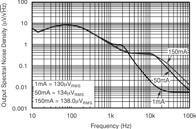
| CIN = 1 μF, COUT = 2.2 μF, VIN = 3.5 V, VOUT(nom) = 3.0 V | ||
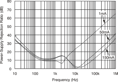
| VIN = 3.5 V, VOUT(nom) = 3.0 V, COUT = 2.2 μF | ||
8.3 System Examples
The TPS783 family is designed to be compatible with low-power microprocessors and microcontrollers such as the TI MSP430. In particular, the ultralow quiescent current allows for the TPS783 family to be used in battery-powered applications.
When the system is active, a voltage supervisor enables the regulator and puts the MSP430 into active mode when there is a battery installed and its voltage is above a certain threshold, as shown in Figure 22. The dashed red line indicates the ground current.
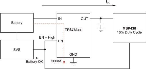 Figure 22. MSP430 Application in Active Mode
When the battery is depleted, the voltage supervisor signals to replace the system battery. After the battery is removed, the voltage supervisor disables the regulator and signals the MSP430 to go into low-power mode. At this moment, the output capacitor functions as a power supply for the MSP430 during the absence of the battery while it is being replaced, as Figure 23 illustrates. The dashed red line indicates the ground current.
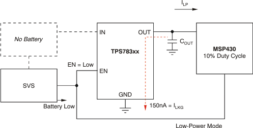 Figure 23. MSP430 Application While Battery is Replaced
Equation 1 shows how to find the required value of the output capacitor (COUT) to provide an appropriate voltage level to the MSP430 for a given amount of time. This time varies from a few seconds to a few minutes, depending on several factors.
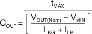
where
- tMAX = maximum time to replace depleted battery
- VOUT(nom) = nominal regulator output equal to initial voltage of capacitor when regulator is disabled
- VMIN = minimum voltage required by MSP430
- I(LKG) = leakage current into regulator output
- I(LP) = current demand from MSP430 in low-power mode
8.3.1 Extending Battery Life in Keep-Alive Circuitry Applications for MSP430 and Other Low-Power Microcontrollers
One of the primary advantages of a low quiescent current LDO is the extremely low energy requirement. Counter-intuitively, this requirement enables a longer battery life compared to using only the battery as an unregulated voltage supply for low-power microcontrollers, such as the MSP430. Figure 24 illustrates the characteristic performance of an unregulated, 3.0-V battery supply versus a regulated TPS783 supply for a typical MSP430 application. Table 2 summarizes this comparison.
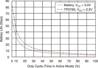
Table 2. Battery Life Comparison vs Active Mode Time for MSP430 Application
| ACTIVE DUTY CYCLE | TPS783xx (NO. OF DAYS) |
BATTERY ONLY (NO. OF DAYS) |
1-μA LDO (NO. OF DAYS) |
|---|---|---|---|
| Active mode, 1 sec/hour (0.028% duty cycle) | 5742 | 6286 | 4373 |
| Active mode, 10 sec/hour (0.28% duty cycle) | 1320 | 998 | 1085 |
| Active mode, 100 sec/hour (2.8% duty cycle) | 151 | 106 | 148 |
| Active mode, 1000 sec/hour (28% duty cycle) | 15.4 | 10.7 | 15.4 |
| Active mode, on all the time (100% duty cycle) | 4.2 | 3.0 | 4.2 |
| CONDITIONS | |||
| Efficiency with VBAT = 3.0 V and VCC = 2.2 V (VOUT/VIN) | 73% | 100% | 73% |
| LDO quiescent current (IQ) | 0.5 μA | 0 | 1 μA |
| MSP430 active current | 2.19 mA | 3.09 mA | 2.19 mA |
| MSP430 low-power current | 0.5 μA | 0.6 μA | 0.5 μA |
8.3.2 Supercapacitor-Based Backup Power
The very-low leakage current at the LDO output provides a system with the flexibility to use the device output capacitor, or supercapacitor, as a temporary backup power supply. The leakage current going into the regulator output from the output capacitor when the LDO is disabled is typically 170 nA; see Figure 10.
8.4 Do's and Don’ts
Do place at least one 1-µF ceramic capacitor as close as possible to the OUT pin of the regulator.
Do not place the output capacitor more than 10 mm away from the regulator.
Do connect a 0.1-μF to 1.0-μF low equivalent series resistance (ESR) capacitor across the IN pin and GND of the regulator.
Do not exceed the absolute maximum ratings.