ZHCSDK5B September 2014 – January 2017 TPS68470
PRODUCTION DATA.
- 1 特性
- 2 应用
- 3 说明
- 4 修订历史记录
- 5 说明 (续)
- 6 Pin Configuration and Functions
- 7 Specifications
-
8 Detailed Description
- 8.1 Overview
- 8.2 Functional Block Diagram
- 8.3
Feature Description
- 8.3.1 Power-Up Sequence and Modes
- 8.3.2 Clock Generation
- 8.3.3 GPIO and Interrupt Generation
- 8.3.4 Sensor GPO Signals
- 8.3.5 Power-Up and Software Reset
- 8.3.6 Core Buck
- 8.3.7 Low Dropout Voltage Regulators (LDOs)
- 8.3.8 WLED Boost Converter and WLED Drivers
- 8.3.9 Indicator LED Operation
- 8.3.10
Safe Operation and Protection Features
- 8.3.10.1 LED Temperature Monitoring (Finger-Burn Protection)
- 8.3.10.2 LED Failure Modes (Open/Short Detection) and Overvoltage Protection
- 8.3.10.3 WLED Open Circuit Detection/Over Voltage Protection
- 8.3.10.4 LED Current Ramp-Up/Down
- 8.3.10.5 Short Circuit Protection
- 8.3.10.6 Hot Die Detection and Thermal Shutdown
- 8.3.11 WLED Boost Inductor Selection
- 8.3.12 I2C Bus Operation
- 8.3.13 Subaddress Definition
- 8.4 Device Functional Modes
- 8.5
Register Map
- 8.5.1 GSTAT Register (address = 0x01) [reset = 00000000]
- 8.5.2 VRSTAT Register (address = 0x02) [reset = -]
- 8.5.3 VRSHORT Register (address = 0x03) [reset = 00000000]
- 8.5.4 INTMASK Register (address = 0x04) [reset = 00000000]
- 8.5.5 VCOSPEED Register (address = 0x05) [reset = 00000000]
- 8.5.6 POSTDIV2 Register (address = 0x06) [reset = 00000000]
- 8.5.7 BOOSTDIV Register (address = 0x07) [reset = 00000000]
- 8.5.8 BUCKDIV Register (address = 0x08) [reset = 00000000]
- 8.5.9 PLLSWR Register (address = 0x09) [reset = 00000000]
- 8.5.10 XTALDIV Register (address = 0x0A) [reset = 00000000]
- 8.5.11 PLLDIV Register (address = 0x0B) [reset = 00000000]
- 8.5.12 POSTDIV Register (address = 0x0C) [reset = 00000000]
- 8.5.13 PLLCTL Register (address = 0x0D) [reset = 10000000]
- 8.5.14 PLLCTL2 Register (address = 0x0E) [reset = 00000000]
- 8.5.15 CLKCFG1 Register (address = 0x0F) [reset = 00000000]
- 8.5.16 CLKCFG2 Register (address = 0x10) [reset = 00000000]
- 8.5.17 GPCTL0A Register (address = 0x14) [reset = 00000001]
- 8.5.18 GPCTL0B Register (address = 0x15) [reset = 00001000]
- 8.5.19 GPCTL1A Register (address = 0x16) [reset = 00000001]
- 8.5.20 GPCTL1B Register (address = 0x17) [reset = 00001000]
- 8.5.21 GPCTL2A Register (address = 0x18) [reset = 00000001]
- 8.5.22 GPCTL2B Register (address = 0x19) [reset = 00001000]
- 8.5.23 GPCTL3A Register (address = 0x1A) [reset = 00000001]
- 8.5.24 GPCTL3B Register (address = 0x1B) [reset = 00001000]
- 8.5.25 GPCTL4A Register (address = 0x1C) [reset = 00000001]
- 8.5.26 GPCTL4B Register (address = 0x1D) [reset = 00001000]
- 8.5.27 GPCTL5A Register (address = 0x1E) [reset = 00000001]
- 8.5.28 GPCTL5B Register (address = 0x1F) [reset = 00001000]
- 8.5.29 GPCTL6A Register (address = 0x20) [reset = 00000001]
- 8.5.30 GPCTL6B Register (address = 0x21) [reset = 00001000]
- 8.5.31 SGPO Register (address = 0x22) [reset = 00000000]
- 8.5.32 PITCTL Register (address = 0x23) [reset = 00000000]
- 8.5.33 WAKECFG Register (address = 0x24) [reset = 00000000]
- 8.5.34 IOWAKESTAT Register (address = 0x25) [reset = 00000000]
- 8.5.35 GPDI Register (address = 0x26) [reset = 00000000]
- 8.5.36 GPDO Register (address = 0x27) [reset = 00000000]
- 8.5.37 ILEDCTL Register (address = 0x28) [reset = 00000000]
- 8.5.38 WLEDSTAT Register (address = 0x29) [reset = 00000000]
- 8.5.39 VWLEDILIM Register (address = 0x2A) [reset = 00001010]
- 8.5.40 VWLEDVAL Register (address = 0x2B) [reset = 00000000]
- 8.5.41 WLEDMAXRER Register (address = 0x2C) [reset = 00000000]
- 8.5.42 WLEDMAXT Register (address = 0x2D) [reset = 00000000]
- 8.5.43 WLEDMAXAF Register (address = 0x2E) [reset = 00000000]
- 8.5.44 WLEDMAXF Register (address = 0x2F) [reset = 00000000]
- 8.5.45 WLEDTO Register (address = 0x30) [reset = 00000000]
- 8.5.46 VWLEDCTL Register (address = 0x31) [reset = 00111000]
- 8.5.47 WLEDTIMER_MSB Register (address = 0x32) [reset = 00000000]
- 8.5.48 WLEDTIMER_LSB Register (address = 0x33) [reset = 00000000]
- 8.5.49 WLEDC1 Register (address = 0x34) [reset = 00000000]
- 8.5.50 WLEDC2 Register (address = 0x35) [reset = 00000000]
- 8.5.51 WLEDCTL Register (address = 0x36) [reset = 00000000]
- 8.5.52 VCMVAL Register (address = 0x3C) [reset = 00000000]
- 8.5.53 VAUX1VAL Register (address = 0x3D) [reset = 00000000]
- 8.5.54 VAUX2VAL Register (address = 0x3E) [reset = 00000000]
- 8.5.55 VIOVAL Register (address = 0x3F) [reset = 00110100]
- 8.5.56 VSIOVAL Register (address = 0x40) [reset = 00110100]
- 8.5.57 VAVAL Register (address = 0x41) [reset = 00000000]
- 8.5.58 VDVAL Register (address = 0x42) [reset = 00000000]
- 8.5.59 S_I2C_CTL Register (address = 0x43) [reset = 00000000]
- 8.5.60 VCMCTL Register (address = 0x44) [reset = 00000000]
- 8.5.61 VAUX1CTL Register (address = 0x45) [reset = 00000000]
- 8.5.62 VAUX2CTL Register (address = 0x46) [reset = 00000000]
- 8.5.63 VACTL Register (address = 0x47) [reset = 00000000]
- 8.5.64 VDCTL Register (address = 0x48) [reset = 00000100]
- 8.5.65 RESET Register (address = 0x50) [reset = N/A]
- 8.5.66 REVID Register (address = 0xFF) [reset = 00100000]
- 9 Application and Implementation
- 10Power Supply Recommendations
- 11Layout
- 12器件和文档支持
- 13机械、封装和可订购信息
9 Application and Implementation
NOTE
Information in the following applications sections is not part of the TI component specification, and TI does not warrant its accuracy or completeness. TI’s customers are responsible for determining suitability of components for their purposes. Customers should validate and test their design implementation to confirm system functionality.
9.1 Application Information
The target application for this device is to power a camera module in portable computers and tablets. The recommendations given in the following section are based on the target application.
9.2 Typical Application
The following figure shows the application schematic for the TPS68470 PMIC. For recommended component values refer to Table 73.
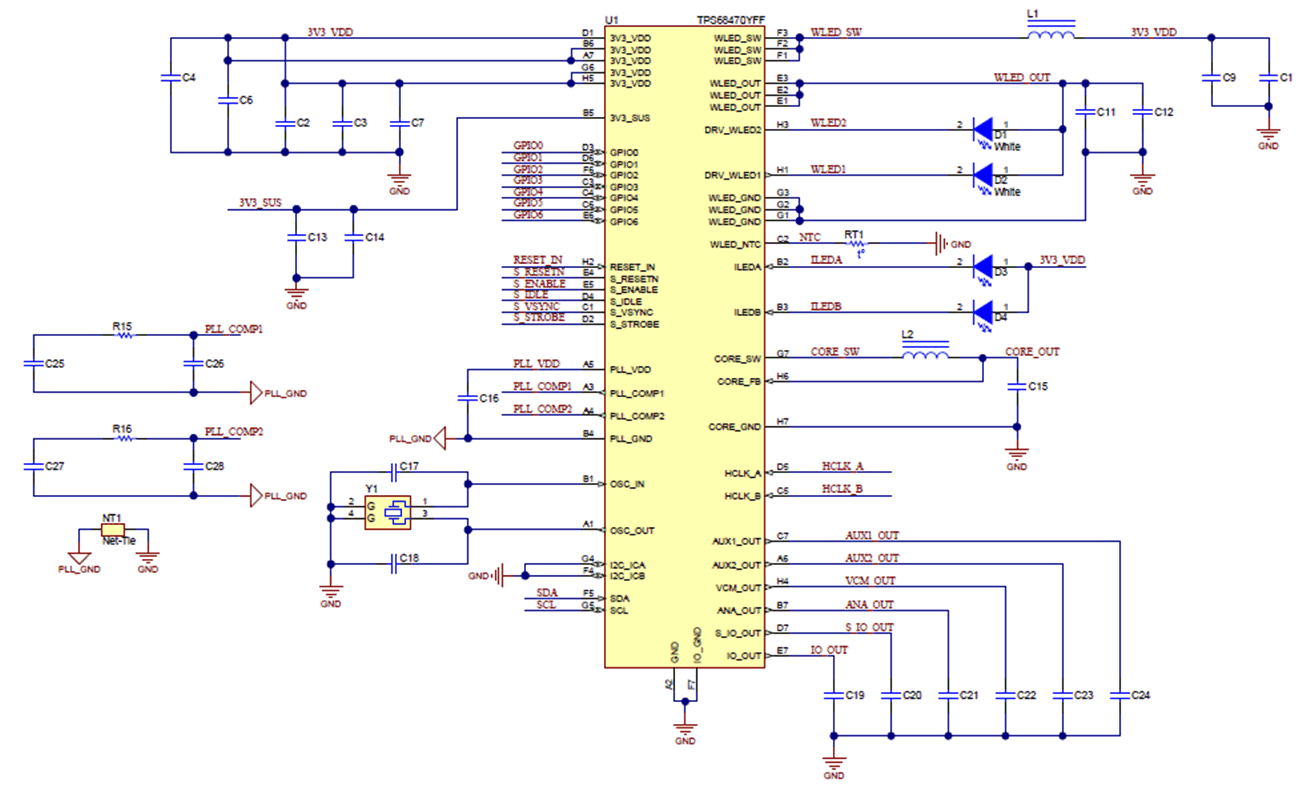 Figure 83. Application Schematic for the TPS68470 (refer to Table 73 for values)
9.2.1 Design Requirements
Table 72. Design Parameters
| PARAMETER | VOLTAGE |
|---|---|
| Input Voltage Range (3V3_VDD and 3V3_SUS) | 3.3V |
| Buck Output Voltage | Default Setting = Off |
| Boost Output Voltage | Default Setting = Off |
| LDO_IO Output Voltage | Default Setting = On (1.8V) |
| LDO_ANA Output Voltage | Default Setting = Off |
| LDO_S_IO Output Voltage | Default Setting = Off |
| LDO_VCM Output Voltage | Default Setting = Off |
| LDO_AUX1 Output Voltage | Default Setting = Off |
| LDO_AUX2 Output Voltage | Default Setting = Off |
9.2.2 Detailed Design Procedure
This section describes the application design procedure for the TPS68470 camera module PMIC. It covers the external component selection for the specified application requirements.
9.2.2.1 Core Buck Design
There are three components required for the buck to operate properly: inductor, output capacitor, and input capacitor. The inductor and output capacitor form an output filter that averages the switch node into a clean regulated supply. The input capacitor supplies the instantaneous current demand of the converter while reducing the noise injected onto the input supply voltage for the other loads.
9.2.2.1.1 Inductor Selection
The CORE_SW pin is the switch node of the converter to which the output inductor is connected. The other end of the inductor connects to the output capacitor.
The inductor value affects the peak-to-peak ripple current, the PFM-to-PWM transition point, the output voltage ripple and the efficiency. In addition, the inductor selected has to be rated for the appropriate saturation current, core losses and DC resistance (DCR). The inductor ripple current decreases with higher inductance and increases with higher VIN. For the CORE buck converter, it is recommended to use an inductor with an inductance range of 1.0 µH to 2.2 μH and with the appropriate current rating for the application.
Use the equation below to calculate the theoretical desired inductance value that fits the application.

Where:
IMAX is the maximum DC load current of the application.
VOUT is the typical output voltage of the voltage rail.
VIN is the input voltage to the converter. For this calculation, use the expected maximum input voltage.
fsw is the typical switching frequency of the converter.
KIND is the desired ripple current divided by IMAX. Typically between 0.2 and 0.4.
LT is the theoretical inductance of the desired inductor.
With the chosen inductance value, the peak current, ILMAX, for the inductor in steady state operation can be calculated using the equations below. The rated saturation current of the inductor must be higher than the ILMAX current.


Where:
ILmax is the maximum current through the inductor.
ILripple is the ripple current through the inductor in PWM mode.
L is the typical inductance of the selected inductor.
In DC/DC converter applications, the efficiency is affected by the inductor core losses and by the inductor DCR value. To achieve high efficiency operation, care should be taken in selecting inductors featuring a low DCR value and low core losses at the typical VIN, VOUT and switching frequency. Increasing the inductor value produces lower ripple and peak currents while increasing efficiency but, degrades transient response. For a given physical inductor size, increased inductance usually results in an inductor with lower saturation current.
At low load currents, the switching and core losses are reduced by the PFM mode feature. The approximate transition point of the converter between PFM and PWM is when the DC load current is equal to 50% of ILripple.
The table at the end of this section lists the recommended inductors for the CORE buck converter.
9.2.2.1.2 Output Capacitor
The output capacitor completes the LC output filter. It is important to chose an output capacitor that suits the application and inductor selection for stabiliblity, output voltage ripple, and specific application requirements such as size and cost. Ceramic capacitors with low ESR values provide the lowest output voltage ripple and are recommended. The output capacitor requires either an X7R or X5R dielectric. Y5V and Z5U dielectric capacitors, aside from their wide variation in capacitance over temperature, become resistive at high frequencies. In order to achieve specified regulation performance and low output voltage ripple, the DC-bias characteristic of ceramic capacitors must be considered. The effective capacitance of ceramic capacitors drops with increasing DC bias voltage.
For the output capacitor of the CORE buck converter, the use of a small ceramic capacitor placed as close as possible to the inductor and the respective CORE_GND pin of the IC is recommended. If, for any reason, the application requires the use of large capacitors which cannot be placed close to the IC, use a smaller ceramic capacitor in parallel to the large capacitor. The small capacitor should be placed as close as possible to the inductor and the respective CORE_GND pin of the IC.
Refer to Table 73 for recommended values.
Use the equation below to calculate the maximum ESR of the output capacitor allowed in-order to meet the maximum output voltage ripple.

Where:
VOUTripple is the maximum output voltage ripple allowed by the application.
RESR is the ESR of the output capacitance.
9.2.2.1.3 Input Capacitor
Due to the nature of the switching converter with a pulsating input current, a low ESR input capacitor is required for best input voltage filtering and minimizing the interference with other circuits caused by high input voltage spikes. To achieve the low ESR requirement, a ceramic capacitor is recommended. However, the voltage rating and DC bias characteristic of ceramic capacitors need to be considered. The input capacitor can be increased without any limit for better input voltage filtering. Be sure to size the ceramic capacitor to achieve the recommended input capacitance. Place the ceramic capacitor as close as possible to the respective 3V3_VDD and CORE_GND pins of the IC.

Where:
ΔVIN is the maximum input voltage ripple allowed by the application.
CIN is the input capacitance.
9.2.2.2 WLED Boost Design
There are three components required for the boost to operate properly: inductor, output capacitor, and input capacitor.
9.2.2.2.1 Inductor Selection
The WLED_SW pin is the switch node of the converter which connects to the inductor of the WLED boost converter. The inductor must be connected between the WLED_SW pin and the input capacitor. Use the equation below to calculate the theoretical desired inductance for the inductor.

Where:
IMAX is the maximum DC load current of the application.
VOUT is the typical output voltage of the voltage rail.
VIN is the input voltage to the converter.
fsw is the typical switching frequency of the boost converter.
KIND is the desired ripple current divided by IMAX. Typically between 0.2 and 0.4.
LT is the theoretical inductance of the desired inductor.
With the chosen inductance value, the peak current, ILMAX, for the inductor in steady state operation can be calculated using the equations below. The rated saturation current of the inductor must be higher than the ILMAX current.


Where:
ILmax is the maximum current through the inductor.
ILripple is the ripple current through the inductor in PWM mode.
L is the typical inductance of the selected inductor.
In DC/DC converter applications, the efficiency is affected by the inductor core losses and by the inductor DCR value. To achieve high efficiency operation, care should be taken in selecting inductors featuring a low DCR value and low core losses at the typical VIN, VOUT and switching frequency. Increasing the inductor value produces lower ripple and peak currents while increasing efficiency but, degrades transient response. For a given physical inductor size, increased inductance usually results in an inductor with lower saturation current.
The table at the end of this section lists the recommended inductors for the WLED boost converter.
9.2.2.2.2 Output Capacitor
It is important to chose an output capacitor that suits the application and inductor selection for stabiliblity, output voltage ripple, and specific application requirements such as size and cost. Ceramic capacitors with low ESR values provide the lowest output voltage ripple and are recommended. The output capacitor requires either an X7R or X5R dielectric. Y5V and Z5U dielectric capacitors, aside from their wide variation in capacitance over temperature, become resistive at high frequencies. In order to achieve specified regulation performance and low output voltage ripple, the DC-bias characteristic of ceramic capacitors must be considered. The effective capacitance of ceramic capacitors drops with increasing DC bias voltage.
For the output capacitor of the boost converter, the use of a small ceramic capacitor placed as close as possible to the inductor and the respective WLED_GND pin of the IC is recommended. If, for any reason, the application requires the use of large capacitors which cannot be placed close to the IC, use a smaller ceramic capacitor in parallel to the large capacitor. The small capacitor should be placed as close as possible to the WLED_OUT pins and the respective WLED_GND pin of the IC.
Use the equation below to calculate the minimum output capacitance with regards to load transient performance.
Refer to Table 73 for recommended values.
9.2.2.2.3 Input Capacitor
Due to the nature of the switching converter with a pulsating input current, a low ESR input capacitor is required for best input voltage filtering and minimizing the interference with other circuits caused by high input voltage spikes. To achieve the low ESR requirement, a ceramic capacitor is recommended. However, the voltage rating and DC bias characteristic of ceramic capacitors need to be considered. The input capacitor can be increased without any limit for better input voltage filtering. Be sure to size the ceramic capacitor to achieve the recommended input capacitance. Place the ceramic capacitor as close as possible to the inductor and WLED_GND pins of the IC.
Refer to Table 73 for recommended values.
9.2.2.3 LDOs Capacitor Selection
It is recommended to use at least 1.0 µF of output capacitance for each LDO output. The input capacitance for each LDO can be combined into one ceramic capacitor of at least 4.7 µF. For both the input and output capacitors, it is recommended to use small ceramic capacitors placed as close as possible to the IC VDD and GND pins. X5R or X7R dielectric capacitors are required for proper operation over temperature.
9.2.2.4 LED Selection
For the indicator LED selection, it is best to chose LEDs with small maximum Vf to maximize LED control head room. A red LED with a maximum Vf of 2.2V is a good choice.
For the WLED selection, it is best to chose a WLED with a maximum current of at least 1A and small to fit the form factor of the application design.
9.2.2.5 Recommended External Components
The following external components are recommended for use with the TPS68470.
Table 73. List of External Components
| BLOCK | COMPONENT | COMPONENT NUMBER | MANUFACTURER | VALUE | SERIES | DIMENSIONS |
|---|---|---|---|---|---|---|
| CORE BUCK | Inductor | L2 | Toko | 1.0 µH | 1269AS-H-1R0M | 2.5 x 2.0 x 1.0 mm |
| Taiyo Yuden | 1.5 µH | CKP2012N1R5M | 2.0 x 1.25 x 1.0 mm | |||
| 1.0 µH | NR3010_1R0 | 3.0 x 3.0 x 1.0 mm | ||||
| Output capacitor | C15 | 4.7 µF | X5R or X7R ceramic capacitor | |||
| Input capacitor | C2 | 10 µF | X5R or X7R ceramic capacitor | |||
| WLED BOOST | Inductor | L1 | TDK | 2.2 µH | SMP3012 | 3.2 x 3.0 x 1.2 mm |
| 2.2 µH | SMP3015 | 3.2 x 3.0 x 1.5 mm | ||||
| 2.2 µH | SMP4012 | 4.4 x 4.1 x 1.2 mm | ||||
| Output capacitor | C11, C12 | 10 µF | X5R or X7R ceramic capacitor | |||
| Input capacitor | C1, C9 | 10 µF | X5R or X7R ceramic capacitor | |||
| WLED | Flash LEDs | D1, D2 | Everlight | ELCH08-5070J6J8284110-N0 | 2.04 x 1.64 x 0.75 mm | |
| All LDO’s | Output capacitor | C19 - C24 | 1.0 µF | X5R or X7R ceramic capacitor | ||
| CLK generator | XTAL | Y1 | Pericom | FL2000044 | 3.2 x 2.5 x 0.65mm | |
| Epson | 24MHz | FA - 128 | 2.0 x 1.6 x 0.5 mm | |||
| TXC | TXC – 7M | 3.2 x 2.5 x 0.7 mm | ||||
| Comp capacitors | C26, C28 | 2.2 nF | X5R or X7R ceramic capacitor | |||
| C25, C27 | 10 nF | X5R or X7R ceramic capacitor | ||||
| Comp resistors | R15, R16 | 8.2 kΩ | ||||
| 3V3_SUS | Supply capacitor | C13 | 4.7 µF | X5R or X7R ceramic capacitor | ||
| Decoupling capacitor | C14 | 0.1 µF | X5R or X7R ceramic capacitor | |||
| 3V3_VDD | Supply capacitors | C3 | 4.7 µF | X5R or X7R ceramic capacitor | ||
| Decoupling capacitor | C4, C6, C7 | 0.1 µF | X5R or X7R ceramic capacitor |
9.2.3 Application Performance Graphs
Table 74. Table of Graphs
| DESCRIPTION | REFERENCE | |
|---|---|---|
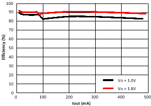
| Core Buck | Efficiency vs. Output Current | Figure 84 |
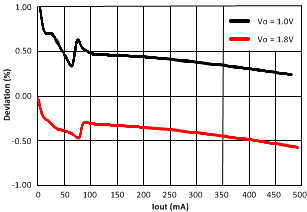
| Load Regulation vs. Output Current | Figure 85 | |
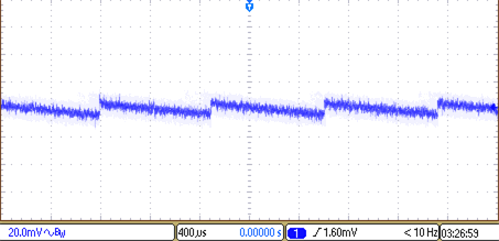
| Output Ripple Voltage, IOUT = 500 mA | Figure 86 | |
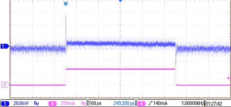
| Load Transient | Figure 87 | |
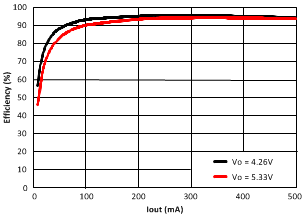
| WLED Boost | Efficiency vs. Output Current | Figure 88 |
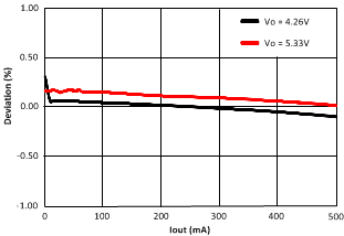
| Load Regulation vs. Output Current | Figure 89 | |
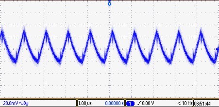
| Output Ripple Voltage, IOUT = 500 mA | Figure 90 | |
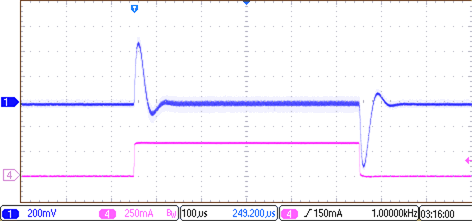
| Load Transient | Figure 91 | |
