ZHCS462A July 2011 – August 2015 TPS65186
PRODUCTION DATA.
- 1 特性
- 2 应用
- 3 说明
- 4 修订历史记录
- 5 说明 (续)
- 6 Pin Configuration and Functions
- 7 Specifications
-
8 Detailed Description
- 8.1 Overview
- 8.2 Functional Block Diagram
- 8.3 Feature Description
- 8.4 Device Functional Modes
- 8.5 Programming
- 8.6
Register Maps
- 8.6.1 Thermistor Readout (TMST_VALUE)
- 8.6.2 Enable (ENABLE)
- 8.6.3 Voltage Adjustment Register (VADJ)
- 8.6.4 VCOM 1 (VCOM1)
- 8.6.5 VCOM 2 (VCOM2)
- 8.6.6 Interrupt Enable 1 (INT_EN1)
- 8.6.7 Interrupt Enable 2 (INT_EN2)
- 8.6.8 Interrupt 1 (INT1)
- 8.6.9 Interrupt 2 (INT2)
- 8.6.10 Power Up Sequence Register 0 (UPSEQ0)
- 8.6.11 Power Up Sequence Register 1 (UPSEQ1)
- 8.6.12 Power Down Sequence Register 0 (DWNSEQ0)
- 8.6.13 Power Down Sequence Register 1 (DWNSEQ1)
- 8.6.14 Thermistor Register 1 (TMST1)
- 8.6.15 Thermistor Register 2 (TMST2)
- 8.6.16 Power Good Status (PG)
- 8.6.17 Revision and Version Control (REVID)
- 9 Application and Implementation
- 10Power Supply Recommendations
- 11Layout
- 12器件和文档支持
- 13机械、封装和可订购信息
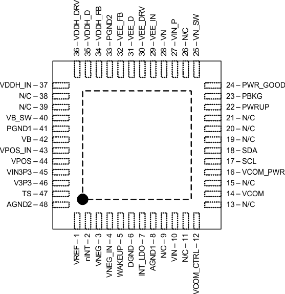
6 Pin Configuration and Functions
RGZ Package
48-Pin VQFN
Top View

Pin Functions
| PIN | I/O | DESCRIPTION | |
|---|---|---|---|
| NAME | NO. | ||
| AGND1 | 8 | — | Analog ground for general analog circuitry |
| AGND2 | 48 | — | Reference point to external thermistor and linearization resistor |
| DGND | 6 | — | Digital ground. Connect to ground plane. |
| INT_LDO | 7 | O | Filter pin for 2.7-V internal supply |
| nINT | 2 | O | Open drain interrupt pin (active low) |
| N/C | 9, 11, 13, 15, 19, 20, 21, 26, 38, 39 | — | Not internally connected |
| PBKG | 23 | — | Die substrate. Connect to VN (–16 V) with short, wide trace. Wide copper trace will improve heat dissipation. |
| PGND1 | 41 | — | Power ground for DCDC1 |
| PGND2 | 33 | — | Power ground for CP1 (VDDH) and CP2 (VEE) charge pumps |
| PWR_GOOD | 24 | O | Open-drain power good output pin. Pin is pulled low when one or more rails are disabled or not in regulation. DCDC1, DCDC2, and VCOM have no effect on this pin.(1) |
| PWRUP | 22 | I | Power-up pin. Pull this pin high to power up all output rails.(1) |
| SCL | 17 | I | Serial interface (I2C) clock input |
| SDA | 18 | I/O | Serial interface (I2C) data input/output |
| TS | 47 | I | Thermistor input pin. Connect a 10-kΩ NTC thermistor and a 43-kΩ linearization resistor between this pin and AGND. |
| V3P3 | 46 | O | Output pin of 3.3-V power switch |
| VB | 42 | I | Feedback pin for boost converter (DCDC1) and supply for VPOS LDO and VDDH charge pump |
| VB_SW | 40 | O | Boost converter switch out (DCDC1) |
| VCOM | 14 | I | Filter pin for panel common-voltage driver |
| VCOM_CTRL | 12 | I | VCOM enable. Pull this pin high to enable the VCOM amplifier. When pin is pulled low and VN is enabled, VCOM discharge is enabled. (3) |
| VCOM_PWR | 16 | I | Internal supply input pin to VCOM buffer. Connect to the output of DCDC2. |
| VDDH_D | 35 | O | Base voltage output pin for positive charge pump (CP1) |
| VDDH_DRV | 36 | O | Driver output pin for positive charge pump (CP1) |
| VDDH_FB | 34 | I | Feedback pin for positive charge pump (CP1) |
| VDDH_IN | 37 | I | Input supply pin for positive charge pump (CP1) |
| VEE_D | 31 | I | Base voltage output pin for negative charge pump (CP2) |
| VEE_DRV | 30 | O | Driver output pin for negative charge pump (CP2) |
| VEE_FB | 32 | I | Feedback pin for negative charge pump (CP2) |
| VEE_IN | 29 | I | Input supply pin for negative charge pump (CP2) (VEE) |
| VIN | 10 | I | Input power supply to general circuitry |
| VIN3P3 | 45 | I | Input pin to 3.3-V power switch |
| VIN_P | 27 | I | Input power supply to inverting buck-boost converter (DCDC2) |
| VN | 28 | I | Feedback pin for inverting buck-boost converter (DCDC2) and supply for VNEG LDO and VEE charge pump |
| VNEG | 3 | O | Negative supply output pin for panel source drivers |
| VNEG_IN | 4 | I | Input pin for LDO2 (VNEG) |
| VN_SW | 25 | O | Inverting buck-boost converter switch out (DCDC2) |
| VREF | 1 | O | Filter pin for 2.25-V internal reference to ADC |
| VPOS | 44 | O | Positive supply output pin for panel source drivers |
| VPOS_IN | 43 | I | Input pin for LDO1 (VPOS) |
| WAKEUP | 5 | I | Wake-up pin (active high). Pull this pin high to wake up from sleep mode. IC accepts I2C commands after WAKEUP pin is pulled high but power rails remain disabled until PWRUP pin is pulled high. (2) |
| PowerPad | — | — | PowerPad, internally connected to PBKG. Connect to VN with short, wide trace. Wide copper trace will improve heat dissipation. PowerPad must not be connected to ground. |
(1) There will be 0-ns of deglitch for PWRx.
(2) There will be 93.75-µs of deglitch for WAKEUP.
(3) There will be 62.52-µs of deglitch for VCOM_CTRL.