ZHCS495C November 2011 – January 2017 TPS65135
PRODUCTION DATA.
7 Detailed Description
7.1 Overview
The TPS65135 device uses a four-switch buck-boost converter topology to generate one negative and one positive output voltage with a single inductor. The device uses a SIMO topology to achieve excellent line transient response, buck-boost mode for both outputs, and high efficiency over the entire output current range. High efficiency over the entire load-current range is implemented by reducing the converter switching frequency under low load conditions. Out-of-audio mode prevents the switching frequency going below 20 kHz.
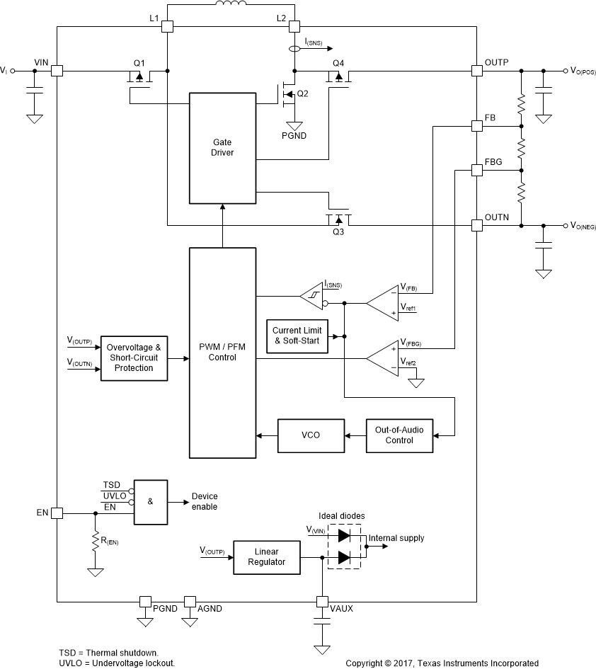
The converter operates with two control loops. One error amplifier controls the positive output voltage VO(POS) so that the FB pin is regulated to 1.24 V. A second error amplifier controls the negative output voltage VO(NEG) so that the FBG pin is regulated to 0 V. An external feedback divider allows both output voltages to be set to the desired value. In principle, the SIMO converter topology operates just like any other buck-boost converter topology, with the difference that the output voltage across the inductor is the sum of the positive and negative output voltages. With this consideration all calculations of the buck-boost converter apply for this topology as well. During the first part of a switching cycle Q1 and Q2 are closed, connecting the inductor from VI to ground. During the second part of a switching cycle, the inductor discharges to the positive and negative outputs by closing switches Q4 and Q3. Because the inductor is discharged to both of the outputs simultaneously, the output voltages can be higher or lower than the input voltage. The converter operates best when the positive output current IO(POS) is equal to the negative output current IO(NEG), for example, as is the case when driving an AMOLED display. However, asymmetries of up to 50% in load current can be canceled out by the used topology. In such cases, a third part of the switching cycle is implemented, during which either Q3 is turned off and Q1 is turned on (as is the case when IO(POS) > IO(NEG)) or Q4 is turned off and Q2 is turned on (as is the case when IO(NEG) > IO(POS)) (see Table 1).
During light loads the converter operates in DCM, using peak-current control and a switching frequ3ency determined by a voltage-controlled oscillator (VCO). At higher load currents the converter operates in CCM with a switching frequency controlled by a fixed off-time. The SIMO regulator topology achieves its best line transient response when operating in DCM.
Table 1. Switch Control
| Switching Cycle | Q1 | Q2 | Q3 | Q4 | Remark |
|---|---|---|---|---|---|
| Part 1 | On | On | Off | Off | |
| Part 2 | Off | Off | On | On | |
| Part 3 | On | Off | Off | On | If IO(POS) > |IO(NEG)| |
| Off | On | On | Off | If |IO(NEG)| > IO(POS) |
7.2 Functional Block Diagram

7.3 Feature Description
7.3.1 Advanced Power-Save Mode for Light-Load Efficiency
In order to maintain high efficiency over the entire load current range, the converter reduces its switching frequency as the load current decreases. The advanced power-save mode controls the switching frequency using a voltage-controlled oscillator (VCO). The VCO frequency is proportional to the inductor peak current, with a lower frequency limit of 20 kHz; but in typical applications the frequency does not go below 100 kHz. This avoids disturbance of the audio band and minimizes audible noise coming from the ceramic input and output capacitors. By maintaining a controlled switching frequency, potential EMI is minimized. This is especially important when using the device in mobile phones. See Figure 24 for typical switching frequency versus load current. For zero load an internal shunt regulator ensures stable output voltage regulation.
7.3.2 Buck-Boost Mode Operation
Buck-boost mode operation allows the input voltage to be higher or lower than the output voltage. This mode allows the use of batteries and supply voltages that are above the positive output voltage.
7.3.3 Inherently Good Line-Transient Regulation
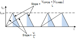
The SIMO regulator achieves inherently good line-transient response when operating in discontinuous conduction mode (DCM), as shown in Figure 14 and Figure 15. In DCM, the current delivered to the output is determined by the peak value and slope of the inductor current. This is illustrated in Figure 7, where the average output current, shown by the shaded area, is the same for different input voltages. Because the converter uses peak-current-mode control, the peak current is fixed as long as the load current is fixed. The falling slope of the inductor current is given by the difference between the positive and negative output voltages and the inductor value; it is independent of the input voltage. As a result, any change in input voltage changes the converter duty cycle but not the peak value or slope of the inductor current when discharging. The average output current, given by the area A (Figure 7), therefore remains constant over any input voltage variation. Entering continuous conduction mode (CCM) linearly decreases the line-transient performance; however, the line-transient response in CCM is still as good as any standard current-mode switching converter.
 Figure 7. Inherently Good Line-Transient Regulation
The following formulas describe the operation of the TPS65135 device when operating in CCM with equal positive and negative output currents. The converter always sees the sum VO of the magnitude of the positive and negative output voltages, as given by
SPACE

where
- VO(POS) is the positive output voltage
- and VO(NEG) is the negative output voltage.
SPACE
The converter duty cycle is calculated using the efficiency estimation from datasheet curves or from real application measurements. A value of 70% for the efficiency η is a good starting assumption for most applications.
SPACE

where
- D is the duty cycle of Q2
- and η is the converter efficiency.
SPACE
Now the output current for entering CCM can be calculated. The switching frequency can be obtained from the data sheet graphs. A frequency of 1.5 MHz is a good assumption for these calculations.
SPACE

where
- IO(CCM) is the value of output current at which continuous conduction starts;
- f is the converter switching frequency;
- and L is the inductance connected between the L1 and L2 pins.
SPACE
The inductor ripple current when operating in CCM can also be calculated
SPACE

where
- I(L)(PP) is the peak-to-peak (that is, ripple) inductor current.
SPACE
Finally, the converter switch peak current can be calculated
SPACE

where
- I(L)M is the peak (that is, maximum) inductor current.
SPACE
7.3.4 Overvoltage Protection
The device monitors the positive and negative output voltages and reduces the current limit when either (or both) of the output voltages exceeds its overvoltage protection threshold. The positive output voltage is clamped to 7 V and the negative output voltage to –7.6 V.
7.3.5 Short-Circuit Protection
Both outputs are protected against short circuits either to ground or to the other output. The device's switching frequency and current limit are reduced in case of a short circuit.
7.3.6 Soft-Start Operation
The device increases the current limit during soft-start operation to avoid high inrush currents during start up. The current limit typically ramps up to its maximum value within 100 µs.
7.3.7 Output-Current Mismatch
The device operates best when the current of the positive output is similar to the current of the negative output. However, the device is able to regulate an output current mismatch of up to 50% (See Figure 26 for typically allowed currents, only 50% mismatch is specified). If the output-current mismatch becomes much larger one of the outputs goes out of regulation and finally the device shuts down. In case of zero load of one output the other output can support up to 5 mA. The device automatically recovers when the mismatch is reduced. The formula below can be used to calculate the maximum supported current mismatch.
SPACE

SPACE
7.3.8 Setting the Output Voltages
The output voltages are set by the three feedback resistors R1, R2, and R3 (Figure 8). R1 and R2 set the positive output voltage VO(POS) and R2 and R3 set the negative output voltage VO(NEG). To reduce the circuit's sensitivity to noise, it is recommended to choose R2 so that a current of at least 10 µA flows through the feedback resistors. Equation 7 can be used to calculate a suitable value for R2.
SPACE

SPACE
The positive output voltage VO(POS) is given by
SPACE

SPACE
The negative output voltage VO(NEG) is given by
SPACE

7.4 Device Functional Modes
7.4.1 Operation with 2.5 V ≤ VI ≤ 5.5 V
The recommended input supply voltage is 2.5 V to 5.5 V. Within this range the device operates normally and achieves its specified performance.
7.4.2 Operation with VI < 2.5 V
The recommended minimum input supply voltage is 2.5 V. The device continues to operate with input supply voltages lower than 2.5 V, however, its performance is not specified. The device does not operate with input supply voltages below the UVLO threshold.
7.4.3 Operation with VI > 5.5 V
The recommended maximum input supply voltage is 5.5 V. As long as the absolute maximum voltage is not exceeded, the device will not be damaged by input supply voltages greater than 5.5 V, however, its performance is not specified.
7.4.4 Operation with EN
When EN = L the device is disabled and switching is inhibited. When EN = H the device is enabled and its start-up sequence begins. If the EN pin is left floating an internal 500-kΩ resistor pulls this pin to ground.