ZHCS495C November   2011  – January 2017 TPS65135

PRODUCTION DATA.  

  1. 特性
  2. 应用
  3. 说明
  4. 修订历史记录
  5. Pin Configuration and Functions
  6. Specifications
    1. 6.1 Absolute Maximum Ratings
    2. 6.2 ESD Ratings
    3. 6.3 Recommended Operating Conditions
    4. 6.4 Thermal Information
    5. 6.5 Electrical Characteristics
    6. 6.6 Typical Characteristics
  7. Detailed Description
    1. 7.1 Overview
    2. 7.2 Functional Block Diagram
    3. 7.3 Feature Description
      1. 7.3.1 Advanced Power-Save Mode for Light-Load Efficiency
      2. 7.3.2 Buck-Boost Mode Operation
      3. 7.3.3 Inherently Good Line-Transient Regulation
      4. 7.3.4 Overvoltage Protection
      5. 7.3.5 Short-Circuit Protection
      6. 7.3.6 Soft-Start Operation
      7. 7.3.7 Output-Current Mismatch
      8. 7.3.8 Setting the Output Voltages
    4. 7.4 Device Functional Modes
      1. 7.4.1 Operation with 2.5 V ≤ VI ≤ 5.5 V
      2. 7.4.2 Operation with VI < 2.5 V
      3. 7.4.3 Operation with VI > 5.5 V
      4. 7.4.4 Operation with EN
  8. Application and Implementation
    1. 8.1 Application Information
    2. 8.2 Typical Application
      1. 8.2.1 Design Requirements
      2. 8.2.2 Detailed Design Procedure
        1. 8.2.2.1 Choosing a Suitable Inductor
        2. 8.2.2.2 Choosing Suitable Input and Output Capacitors
        3. 8.2.2.3 Choosing Suitable Feedback Resistors
        4. 8.2.2.4 Measurement Circuit
      3. 8.2.3 Application Curves
  9. Power Supply Recommendations
  10. 10Layout
    1. 10.1 Layout Guidelines
    2. 10.2 Layout Example
  11. 11器件和文档支持
    1. 11.1 器件支持
      1. 11.1.1 Third-Party Products Disclaimer
    2. 11.2 接收文档更新通知
    3. 11.3 社区资源
    4. 11.4 商标
    5. 11.5 静电放电警告
    6. 11.6 Glossary
  12. 12机械、封装和可订购信息

封装选项

机械数据 (封装 | 引脚)
散热焊盘机械数据 (封装 | 引脚)
订购信息

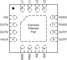
Pin Configuration and Functions

RTE Package
16-Pin WQFN
Top View
TPS65135 PinOut_01_SLVS704.gif

Pin Functions

PIN I/O DESCRIPTION
NAME NO.
EN 8 I Input pin to enable the device. Pulling this pin high enables the device. This pin has an internal 500-kΩ pull-down resistor.
FB 7 I Feedback regulation point for the positive output voltage rail
FBG 6 I Feedback regulation point for the negative output voltage rail
GND 5 Analog ground
L1 15 I/O Inductor terminal
16
L2 13 I/O Inductor terminal
14
OUTN 2 O Negative output
3
OUTP 9 O Positive output
10
PGND 11 Power ground
12
VAUX 4 I/O Reference voltage output. This pin requires a 100-nF capacitor for stability.
VIN 1 I Input supply
Exposed thermal pad Connect this pad to ground