ZHCSFX4 December 2016 TPS63027
PRODUCTION DATA.
- 1 特性
- 2 应用范围
- 3 说明
- 4 典型应用
- 5 修订历史记录
- 6 Device Comparison Table
- 7 Pin Configuration and Functions
- 8 Specifications
- 9 Detailed Description
- 10Application and Implementation
- 11Power Supply Recommendations
- 12Layout
- 13器件和文档支持
- 14机械、封装和可订购信息
9 Detailed Description
9.1 Overview
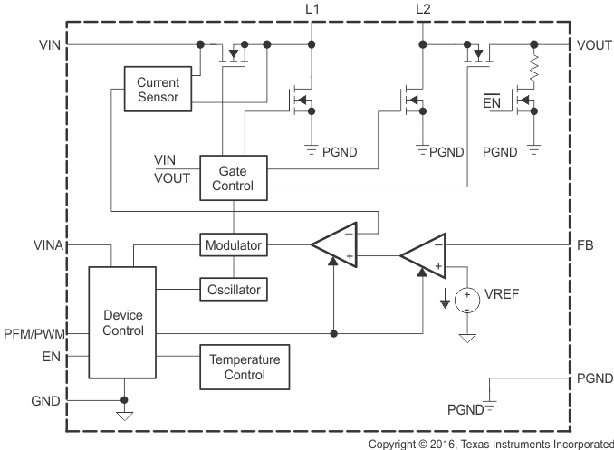
The TPS63027 use 4 internal N-channel MOSFETs to maintain synchronous power conversion at all possible operating conditions. This enables the device to keep high efficiency over the complete input voltage and output power range. To regulate the output voltage at all possible input voltage conditions, the device automatically switches from buck operation to boost operation and back as required by the configuration. It always uses one active switch, one rectifying switch, one switch is held on, and one switch held off. Therefore, it operates as a buck converter when the input voltage is higher than the output voltage, and as a boost converter when the input voltage is lower than the output voltage. There is no mode of operation in which all 4 switches are switching at the same time. Keeping one switch on and one switch off eliminates their switching losses. The RMS current through the switches and the inductor is kept at a minimum, to minimize switching and conduction losses. Controlling the switches this way allows the converter to always keep higher efficiency.
The device provides a seamless transition from buck to boost or from boost to buck operation.
9.2 Functional Block Diagram

9.3 Feature Description
9.3.1 Undervoltage Lockout (UVLO)
To avoid mis-operation of the device at low input voltages, an undervoltage lockout is included. UVLO shuts down the device at low input voltages to ensure proper operation. See eletrical characteristics table for the dedicated values.
9.3.2 Output Discharge Function
When the device is disabled by pulling enable low and the supply voltage is still applied, the internal transistor use to discharge the output capacitor is turned on, and the output capacitor is discharged until UVLO is reached. This means, if there is no supply voltage applied the output discharge function is also disabled. The transistor which is responsible of the discharge function, when turned on, operates like an equivalent 120-Ω resistor, ensuring typically less than 10ms discharge time for 20-µF output capacitance and a 3.3 V output.
9.3.3 Thermal Shutdown
The device goes into thermal shutdown once the junction temperature exceeds typically 140°C with a 20°C hysteresis.
9.3.4 Softstart
To minimize inrush current and output voltage overshoot during start up, the device has a Softstart. At turn on, the input current raises monotonic until the output voltage reaches regulation. During Softstart, the input current follows the current ramp charging the internal Softstart capacitor. The device smoothly ramps up the input current bringing the output voltage to its regulated value even if a large capacitor is connected at the output.
The Softstart time is measured as the time from when the EN pin is asserted to when the output voltage has reached 90% of its nominal value. There is a delay time from when the EN pin is asserted to when the device starts the switching activity. The Softstart time depends on the load current, the input voltage, and the output capacitor. The Softstart time in boost mode is longer then the time in buck mode.
The inductor current is able to increase and always assure a soft start unless a real short circuit is applied at the output.
9.3.5 Short Circuit Protection
The TPS63027 provides short circuit protection to protect itself and the application. When the output voltage does not increase above 1.2V, the device assumes a short circuit at the output and limits the input current to 4 A.
9.4 Device Functional Modes
9.4.1 Control Loop Description
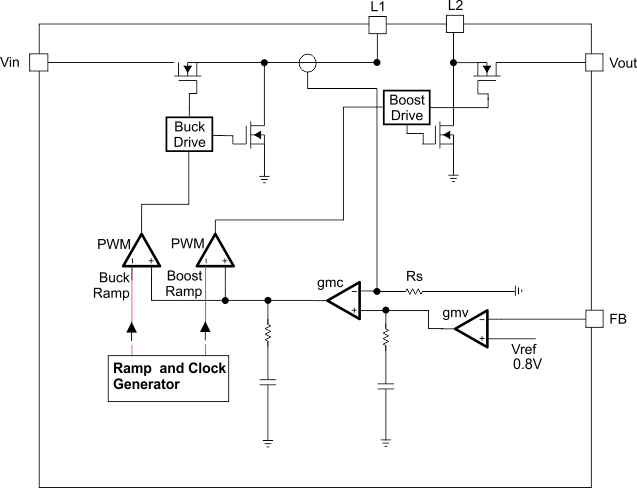
 Figure 3. Average Current Mode Control
The controller circuit of the device is based on an average current mode topology. The average inductor current is regulated by a fast current regulator loop which is controlled by a voltage control loop. Figure 3 shows the control loop.
The non inverting input of the transconductance amplifier, gmv, is assumed to be constant. The output of gmv defines the average inductor current. The inductor current is reconstructed by measuring the current through the high side buck MOSFET. This current corresponds exactly to the inductor current in boost mode. In buck mode the current is measured during the on time of the same MOSFET. During the off time, the current is reconstructed internally starting from the peak value at the end of the on time cycle. The average current and the feedback from the error amplifier gmv forms the correction signal gmc. This correction signal is compared to the buck and the boost sawtooth ramp giving the PWM signal. Depending on which of the two ramps the gmc output crosses either the Buck or the Boost stage is initiated. When the input voltage is close to the output voltage, one buck cycle is always followed by a boost cycle. In this condition, no more than three cycles in a row of the same mode are allowed. This control method in the buck-boost region ensures a robust control and the highest efficiency.
9.4.2 Power Save Mode Operation
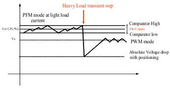
 Figure 4. Power Save Mode Operation
Depending on the load current, in order to provide the best efficiency over the complete load range, the device works in PWM mode at load currents of typically 350mA or higher. At lighter loads, the device switches automatically into Power Save Mode to reduce power consumption and extend battery life. The MODE pin is used to select between the two different operation modes. To enable Power Save Mode, the MODE pin must be set HIGH.
During Power Save Mode, the part operates with a reduced switching frequency and lowest supply current to maintain high efficiency. The output voltage is monitored with a comparator at every clock cycle by the thresholds comp low and comp high. When the device enters Power Save Mode, the converter stops operating and the output voltage drops. The slope of the output voltage depends on the load and the output capacitance. When the output voltage reaches the comp low threshold, at the next clock cycle the device ramps up the output voltage again, by starting operation. Operation can last for one or several pulses until the comp high threshold is reached. At the next clock cycle, if the load is still lower than about 350mA, the device switches off again and the same operation is repeated. Instead, if at the next clock cycle, the load is above 350mA, the device automatically switches to PWM mode.
In order to keep high efficiency in PFM mode, there is only one comparator active to keep the output voltage regulated. The AC ripple in this condition is increased, compared to the PWM mode. The amplitude of this voltage ripple is typically 30 mV pk-pk, with 2-µF effective output capacitance. In order to avoid a critical voltage drop when switching from 0A to full load, the output voltage in PFM mode is typically 1.3% above the nominal value in PWM mode. This is called Dynamic Voltage Positioning and allows the converter to operate with a small output capacitor and still have a low absolute voltage drop during heavy load transients.
Power Save Mode is disabled by setting the MODE pin LOW.
9.4.3 Current Limit
The current limit variation depends on the difference between the input and output voltage. The maximum current limit value is at the highest difference.
Given the curves provided in Figure 6, it is possible to calculate the output current reached in boost mode, using Equation 1 and Equation 2 and in buck mode using Equation 3 and Equation 4.

![TPS63027 TPS63027 q1_boost_lvsa92[1].gif](/ods/images/ZHCSFX4/q1_boost_lvsa92[1].gif)

![TPS63027 TPS63027 q1_buck_lvsa92[1].gif](/ods/images/ZHCSFX4/q1_buck_lvsa92[1].gif)
where
- η = Estimated converter efficiency (use the number from the efficiency curves or 0.90 as an assumption)
- IIN= Minimum average input current (Figure 6)
9.4.4 Supply and Ground
The TPS63027 provides two input pins (VIN and AVIN) and two ground pins (GND and AGND).
The VIN pin supplies the input power, while the AVIN pin provides voltage for the control circuits. A similar approach is used for the ground pins. AGND and GND are used to avoid ground shift problems due to the high currents in the switches. The reference for all control functions is the AGND pin. The power switches are connected to GND. Both grounds must be connected on the PCB at only one point, ideally, close to the AGND pin.
9.4.5 Device Enable
The device starts operation when the EN pin is set high. The device enters shutdown mode when the EN pin is set low. In shutdown mode, the regulator stops switching, all internal control circuitry is switched off, and the load is disconnected from the input.