ZHCSO68 March   2022 TPS629203

PRODUCTION DATA  

  1. 特性
  2. 应用
  3. 说明
  4. Revision History
  5. Device Comparison Table
  6. Pin Configuration and Functions
  7. Specifications
    1. 7.1 Absolute Maximum Ratings
    2. 7.2 ESD Ratings
    3. 7.3 Recommended Operating Conditions
    4. 7.4 Thermal Information
    5. 7.5 Electrical Characteristics
    6. 7.6 Typical Characteristics
  8. Detailed Description
    1. 8.1 Overview
    2. 8.2 Functional Block Diagram
    3. 8.3 Feature Description
      1. 8.3.1 Mode Selection and Device Configuration (MODE/S-CONF Pin)
      2. 8.3.2 Adjustable VO Operation (External Voltage Divider)
      3. 8.3.3 Selectable VO Operation (VSET and Internal Voltage Divider)
      4. 8.3.4 Smart Enable with Precise Threshold
      5. 8.3.5 Power Good (PG)
      6. 8.3.6 Output Discharge Function
      7. 8.3.7 Undervoltage Lockout (UVLO)
      8. 8.3.8 Current Limit and Short Circuit Protection
      9. 8.3.9 Thermal Shutdown
    4. 8.4 Device Functional Modes
      1. 8.4.1 Forced Pulse Width Modulation (PWM) Operation
      2. 8.4.2 Power Save Mode Operation (Auto PFM/PWM)
      3. 8.4.3 AEE (Automatic Efficiency Enhancement)
      4. 8.4.4 100% Duty-Cycle Operation
      5. 8.4.5 Starting into a Prebiased Load
  9. Application and Implementation
    1. 9.1 Application Information
    2. 9.2 Typical Application
      1. 9.2.1 Design Requirements
      2. 9.2.2 Detailed Design Procedure
        1. 9.2.2.1 Custom Design With WEBENCH® Tools
        2. 9.2.2.2 Programming the Output Voltage
        3. 9.2.2.3 External Component Selection
          1. 9.2.2.3.1 Output Filter and Loop Stability
          2. 9.2.2.3.2 Inductor Selection
          3. 9.2.2.3.3 Capacitor Selection
            1. 9.2.2.3.3.1 Output Capacitor
            2. 9.2.2.3.3.2 Input Capacitor
      3. 9.2.3 Application Curves
    3. 9.3 System Examples
      1. 9.3.1 Powering Multiple Loads
      2. 9.3.2 Inverting Buck-Boost (IBB)
  10. 10Power Supply Recommendations
  11. 11Layout
    1. 11.1 Layout Guidelines
    2. 11.2 Layout Example
      1. 11.2.1 Thermal Considerations
  12. 12Device and Documentation Support
    1. 12.1 Device Support
      1. 12.1.1 第三方产品免责声明
      2. 12.1.2 Development Support
        1. 12.1.2.1 Custom Design With WEBENCH® Tools
    2. 12.2 Documentation Support
      1. 12.2.1 Related Documentation
    3. 12.3 接收文档更新通知
    4. 12.4 支持资源
    5. 12.5 Trademarks
    6. 12.6 Electrostatic Discharge Caution
    7. 12.7 术语表
  13. 13Mechanical, Packaging, and Orderable Information

封装选项

机械数据 (封装 | 引脚)
散热焊盘机械数据 (封装 | 引脚)
订购信息

Forced Pulse Width Modulation (PWM) Operation

The TPS629203 has two operating modes: forced PWM mode discussed in this section and auto PFM/PWM mode as discussed in Section 8.4.2.

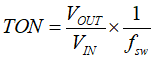
With the MODE/S-CONF pin set to forced PWM mode, the device operates with pulse width modulation in continuous conduction mode (CCM) with a nominal switching frequency of either 1.0 MHz or 2.5 MHz. The frequency variation in PWM is controlled and depends on VIN, VOUT, and the inductance. The on time in forced PWM mode is given by Equation 3.

Equation 3. GUID-20201118-CA0I-WXRM-XD5K-HTMKBG3VSQHD-low.gif

For very small output voltages, an absolute minimum on time of about 40 ns is kept to limit switching losses. The operating frequency is thereby reduced from its nominal value, which keeps efficiency high.