ZHCSO68 March 2022 TPS629203
PRODUCTION DATA
- 1 特性
- 2 应用
- 3 说明
- 4 Revision History
- 5 Device Comparison Table
- 6 Pin Configuration and Functions
- 7 Specifications
-
8 Detailed Description
- 8.1 Overview
- 8.2 Functional Block Diagram
- 8.3
Feature Description
- 8.3.1 Mode Selection and Device Configuration (MODE/S-CONF Pin)
- 8.3.2 Adjustable VO Operation (External Voltage Divider)
- 8.3.3 Selectable VO Operation (VSET and Internal Voltage Divider)
- 8.3.4 Smart Enable with Precise Threshold
- 8.3.5 Power Good (PG)
- 8.3.6 Output Discharge Function
- 8.3.7 Undervoltage Lockout (UVLO)
- 8.3.8 Current Limit and Short Circuit Protection
- 8.3.9 Thermal Shutdown
- 8.4 Device Functional Modes
- 9 Application and Implementation
- 10Power Supply Recommendations
- 11Layout
- 12Device and Documentation Support
- 13Mechanical, Packaging, and Orderable Information
8.4.2 Power Save Mode Operation (Auto PFM/PWM)
When the MODE/S-CONF pin is configured for auto PFM/PWM mode, power save mode is allowed. The device operates in PWM mode as long the output current is higher than half the ripple current of the inductor. To maintain high efficiency at light loads, the device enters power save mode at the boundary to discontinuous conduction mode (DCM). This happens if the output current becomes smaller than half the ripple current of the inductor. Power save mode is entered seamlessly to make sure there is high efficiency in light-load operation. The device remains in power save mode as long as the inductor current is discontinuous.
In power save mode, the switching frequency decreases linearly with the load current maintaining high efficiency. The transition into and out of power save mode is seamless in both directions.
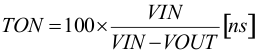
The TPS629203 adjusts the on time (TON) in power save mode, depending on the input voltage and the output voltage to maintain highest efficiency. The on time in steady-state operation can be estimated as:
With the MODE/S-CONF pin set to 1.0-MHz operation:

With the MODE/S-CONF pin set to 2.5-MHz operation:
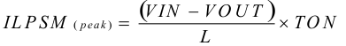
Using TON, the typical peak inductor current in power save mode is approximated by:
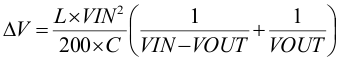
The output voltage ripple in power save mode is given by Equation 7:
When VIN decreases to typically 15% above VOUT, the device will not enter power save mode regardless of the load current. The device maintains output regulation in PWM mode.