ZHCSNV7A March 2020 – December 2021 TPS62816-Q1
PRODUCTION DATA
- 1 特性
- 2 应用
- 3 说明
- 4 Revision History
- 5 Device Comparison Table
- 6 Pin Configuration and Functions
- 7 Specifications
- 8 Parameter Measurement Information
- 9 Detailed Description
- 10Application and Implementation
- 11Power Supply Recommendations
- 12Layout
- 13Device and Documentation Support
- 14Mechanical, Packaging, and Orderable Information
10.2.3 Application Curves
All plots have been taken with a nominal switching frequency of 2.25 MHz
when set to PWM mode, unless otherwise noted. The BOM is according to Table 8-1.
All plots have been taken with a nominal switching frequency of 2.25 MHz
when set to PWM mode, unless otherwise noted. The BOM is according to Table 8-1.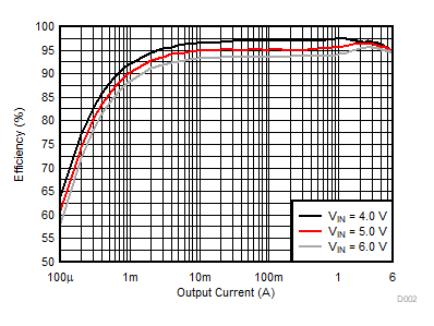
Figure 10-2 Efficiency Versus Output Current. All plots have been taken with a nominal switching frequency of 2.25 MHz
when set to PWM mode, unless otherwise noted. The BOM is according to Table 8-1.

| VOUT = 3.3 V | PFM | TA = 25°C |
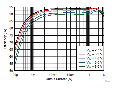
| VOUT = 1.8 V | PFM | TA = 25°C |
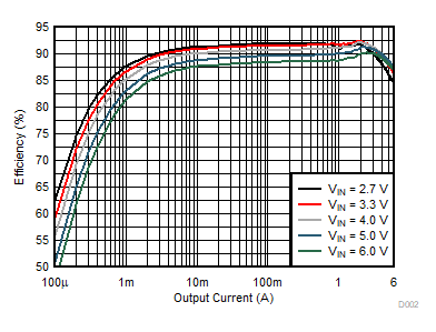
| VOUT = 1.2 V | PFM | TA = 25°C |
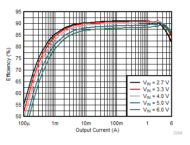
| VOUT = 1.0 V | PFM | TA = 25°C |
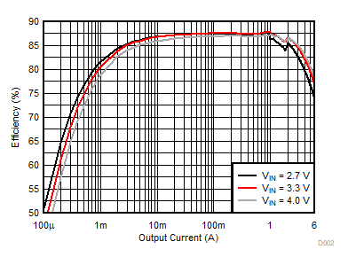
| VOUT = 0.6 V | PFM | TA = 25°C |
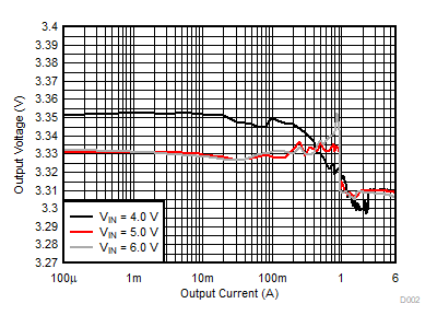
| VOUT = 3.3 V | PFM | TA = 25°C |
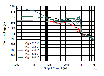
| VOUT = 1.8 V | PFM | TA = 25°C |
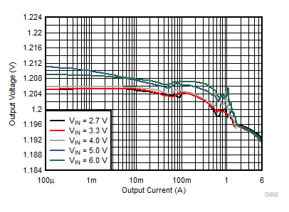
| VOUT = 1.2 V | PFM | TA = 25°C |
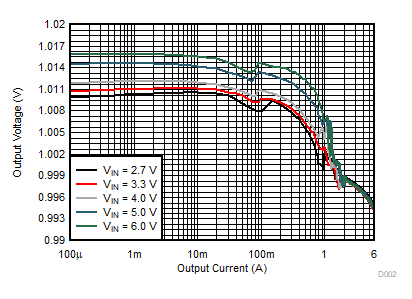
| VOUT = 1.0 V | PFM | TA = 25°C |
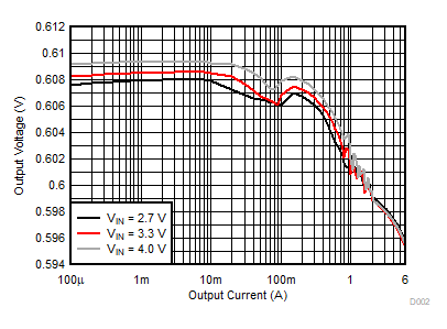
| VOUT = 0.6 V | PFM | TA = 25°C |
| VOUT = 3.3 V | PFM | TA = 25°C |
| VIN = 5.0 V | IOUT = 0.6 A to 5.4 A to 0.6 A | |
| VOUT = 1.8 V | PFM | TA = 25°C |
| VIN = 5.0 V | IOUT = 0.6 A to 5.4 A to 0.6 A | |
| VOUT = 1.2 V | PFM | TA = 25°C |
| VIN = 5.0 V | IOUT = 0.6 A to 5.4 A to 0.6 A | |
| VOUT = 1.0 V | PFM | TA = 25°C |
| VIN = 5.0 V | IOUT = 0.6 A to 5.4 A to 0.6 A | |
| VOUT = 0.6 V | PFM | TA = 25°C |
| VIN = 3.3 V | IOUT = 0.6 A to 5.4 A to 0.6 A | |
| VOUT = 3.3 V | PFM | TA = 25°C |
| IOUT = 0.2 A | VIN = 4.5 V to 5.5 V to 4.5 V | |
| VOUT = 1.8 V | PFM | TA = 25°C |
| IOUT = 0.2 A | VIN = 4.5 V to 5.5 V to 4.5 V | |
| VOUT = 1.2 V | PFM | TA = 25°C |
| IOUT = 0.2 A | VIN = 4.5 V to 5.5 V to 4.5 V | |
| VOUT = 1.0 V | PFM | TA = 25°C |
| IOUT = 0.2 A | VIN = 4.5 V to 5.5 V to 4.5 V | |
| VOUT = 0.6 V | PFM | TA = 25°C |
| IOUT = 0.2 A | VIN = 3.0 V to 3.6 V to 3.0 V | |
| VOUT = 3.3 V | PFM | TA = 25°C |
| VIN = 5 V | IOUT = 0.2 A |
| VOUT = 1.8 V | PFM | TA = 25°C |
| VIN = 5 V | IOUT = 0.2 A |
| VOUT = 1.2 V | PFM | TA = 25°C |
| VIN = 5 V | IOUT = 0.2 A |
| VOUT = 1.0 V | PFM | TA = 25°C |
| VIN = 5 V | IOUT = 0.2 A |
| VOUT = 0.6 V | PFM | TA = 25°C |
| VIN = 3.3 V | IOUT = 0.2 A |
| VOUT = 3.3 V | PWM or PFM | TA = 25°C |
| VIN = 5 V | CSS = 15 nF | IOUT = 6 A |
| VOUT = 1.2 V | PWM or PFM | TA = 25°C |
| VIN = 5 V | CSS = 15 nF | IOUT = 6 A |
| VOUT = 0.6 V | PWM or PFM | TA = 25°C | ||
| VIN = 3.3 V | CSS = 15 nF | IOUT = 6 A |
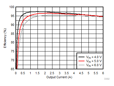
| VOUT = 3.3 V | PWM | TA = 25°C |
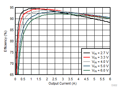
| VOUT = 1.8 V | PWM | TA = 25°C |
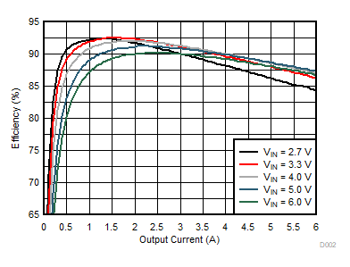
| VOUT = 1.2 V | PWM | TA = 25°C |
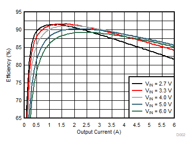
| VOUT = 1.0 V | PWM | TA = 25°C |
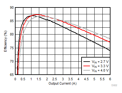
| VOUT = 0.6 V | PWM | TA = 25°C |
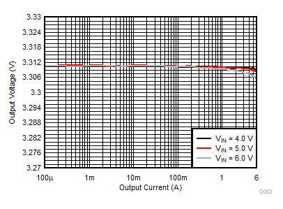
| VOUT = 3.3 V | PWM | TA = 25°C |
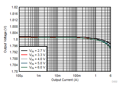
| VOUT = 1.8 V | PWM | TA = 25°C |
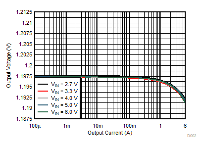
| VOUT = 1.2 V | PWM | TA = 25°C |
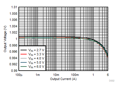
| VOUT = 1.0 V | PWM | TA = 25°C |
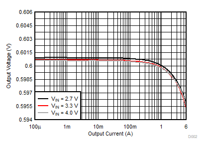
| VOUT = 0.6 V | PWM | TA = 25°C |
| VOUT = 3.3 V | PWM | TA = 25°C |
| VIN = 5.0 V | IOUT = 0.6 A to 5.4 A to 0.6 A | |
| VOUT = 1.8 V | PWM | TA = 25°C |
| VIN = 5.0 V | IOUT = 0.6 A to 5.4 A to 0.6 A | |
| VOUT = 1.2 V | PWM | TA = 25°C |
| VIN = 5.0 V | IOUT = 0.6 A to 5.4 A to 0.6 A | |
| VOUT = 1.0 V | PWM | TA = 25°C |
| VIN = 5.0 V | IOUT = 0.6 A to 5.4 A to 0.6 A | |
| VOUT = 0.6 V | PWM | TA = 25°C |
| VIN = 3.3 V | IOUT = 0.6 A to 5.4 A to 0.6 A | |
| VOUT = 3.3 V | PWM | TA = 25°C |
| IOUT = 6 A | VIN = 4.5 V to 5.5 V to 4.5 V | |
| VOUT = 1.8 V | PWM | TA = 25°C |
| IOUT = 6 A | VIN = 4.5 V to 5.5 V to 4.5 V | |
| VOUT = 1.2 V | PWM | TA = 25°C |
| IOUT = 6 A | VIN = 4.5 V to 5.5 V to 4.5 V | |
| VOUT = 1.0 V | PWM | TA = 25°C |
| IOUT = 6 A | VIN = 4.5 V to 5.5 V to 4.5 V | |
| VOUT = 0.6 V | PWM | TA = 25°C |
| IOUT = 6 A | VIN = 3.0 V to 3.6 V to 3.0 V | |
| VOUT = 3.3 V | PWM | TA = 25°C |
| VIN = 5 V | IOUT = 6 A |
| VOUT = 1.8 V | PWM | TA = 25°C |
| VIN = 5 V | IOUT = 6 A |
| VOUT = 1.2 V | PWM | TA = 25°C |
| VIN = 5 V | IOUT = 6 A |
| VOUT = 1.0 V | PWM | TA = 25°C |
| VIN = 5 V | IOUT = 6 A |
| VOUT = 0.6 V | PWM | TA = 25°C |
| VIN = 3.3 V | IOUT = 6 A |
| VOUT = 1.8 V | PWM or PFM | TA = 25°C |
| VIN = 5 V | CSS = 15 nF | IOUT = 6 A |
| VOUT = 1.0 V | PWM or PFM | TA = 25°C |
| VIN = 5 V | CSS = 15 nF | IOUT = 6 A |