ZHCSIN0K August 2018 – July 2025 TPS62810-Q1 , TPS62811-Q1 , TPS62812-Q1 , TPS62813-Q1
PRODUCTION DATA
8.4.7 软启动/跟踪 (SS/TR)
内部软启动电路控制启动期间的输出电压斜率。该控制可以避免过大的浪涌电流并确保受控的输出电压上升时间。该控制还可防止高阻抗电源或电池产生不必要的压降。当 EN 设置为高电平以开始运行时,器件在一段约 200μs 的延迟后开始切换,然后内部基准和 VOUT 以通过连接至 SS/TR 引脚的外部电容器控制的斜率上升。
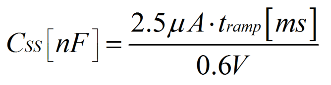
将 SS/TR 引脚保持未连接状态可提供超快的启动斜升(通常为 150µs)。在软启动期间,SS/TR 与 GND 之间连接的电容器以 2.5 µA 通过内部电流源进行充电,直到达到 0.6V 的基准电压。因此,设置特定斜坡时间 (tramp) 所需的电容是:
如果器件设置为关断 (EN = GND)、欠压锁定或热关断,则内部电阻器会将 SS/TR 引脚下拉至 GND,以便确保处于适当的低电平。从这些状态返回会导致新的启动序列。
施加在 SS/TR 上的电压可用于跟踪控制器电压。在强制 PWM 模式下,输出电压在两个方向上跟随此电压上升和下降。在 PFM 模式下,输出电压随负载电流而降低。SS/TR 引脚不得连接到其他器件的 SS/TR 引脚。施加在 SS/TR 上的外部电压被在内部钳位到反馈电压 (0.6V)。TI 建议将 SS/TR 上的外部电压目标设置为略高于反馈电压。考虑到 SS/TR 上的电阻分压器 R5 和 R6 的容差,该操作可确保在上电时序控制完成后,器件会切换到 内部基准电压。请参阅图 9-58。