ZHCSHS6E November   2017  – November 2021 TPS62088 , TPS62088A , TPS62089A

PRODUCTION DATA  

  1. 特性
  2. 应用
  3. 说明
  4. Revision History
  5. Device Options
  6. Pin Configuration and Functions
  7. Specifications
    1. 7.1 Absolute Maximum Ratings 
    2. 7.2 ESD Ratings
    3. 7.3 Recommended Operating Conditions
    4. 7.4 Thermal Information 
    5. 7.5 Electrical Characteristics
    6. 7.6 Typical Characteristics
  8. Detailed Description
    1. 8.1 Overview
    2. 8.2 Functional Block Diagram
    3. 8.3 Feature Description
      1. 8.3.1 Power Save Mode
      2. 8.3.2 Pulse Width Modulation (PWM) Operation
      3. 8.3.3 100% Duty Cycle Low Dropout Operation
      4. 8.3.4 Soft Start
      5. 8.3.5 Switch Current Limit and HICCUP Short-Circuit Protection
      6. 8.3.6 Undervoltage Lockout
      7. 8.3.7 Thermal Shutdown
    4. 8.4 Device Functional Modes
      1. 8.4.1 Enable and Disable
      2. 8.4.2 Power Good
  9. Application and Implementation
    1. 9.1 Application Information
    2. 9.2 Typical Application
      1. 9.2.1 Design Requirements
      2. 9.2.2 Detailed Design Procedure
        1. 9.2.2.1 Custom Design With WEBENCH® Tools
        2. 9.2.2.2 Setting The Output Voltage
        3. 9.2.2.3 Feedforward Capacitor
        4. 9.2.2.4 Output Filter Design
        5. 9.2.2.5 Inductor Selection
        6. 9.2.2.6 Capacitor Selection
      3. 9.2.3 Application Curves
  10. 10Power Supply Recommendations
  11. 11Layout
    1. 11.1 Layout Guidelines
    2. 11.2 Layout Example
      1. 11.2.1 Thermal Considerations
  12. 12Device and Documentation Support
    1. 12.1 Device Support
      1. 12.1.1 第三方产品免责声明
      2. 12.1.2 Development Support
        1. 12.1.2.1 Custom Design With WEBENCH® Tools
    2. 12.2 Documentation Support
      1. 12.2.1 Related Documentation
    3. 12.3 接收文档更新通知
    4. 12.4 支持资源
    5. 12.5 Trademarks
    6. 12.6 Electrostatic Discharge Caution
    7. 12.7 术语表
  13. 13Mechanical, Packaging, and Orderable Information

封装选项

请参考 PDF 数据表获取器件具体的封装图。

机械数据 (封装 | 引脚)
  • YWC|6
  • YFP|6
散热焊盘机械数据 (封装 | 引脚)
订购信息

Pin Configuration and Functions

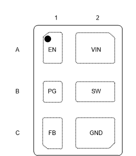
GUID-FC96021D-DC45-408E-932B-C1577B234D1F-low.gifFigure 6-1 YFP PackageTop View
GUID-298FF625-21BC-4F56-A67C-C7485D425CB1-low.gifFigure 6-2 YWC PackageTop View
Table 6-1 Pin Functions
PIN I/O DESCRIPTION
NAME NO.
EN A1 I Device enable pin. To enable the device, this pin needs to be pulled high. Pulling this pin low disables the device. Do not leave floating.
PG B1 O Power-good open-drain output pin. The pullup resistor can be connected to voltages up to 5.5 V. If unused, leave it floating.
FB C1 I Feedback pin. For the fixed output voltage versions, this pin must be connected to the output.
GND C2 Ground pin
SW B2 O Switch pin of the power stage
VIN A2 I Input voltage pin