ZHCSD80B january 2015 – august 2023 TPS62065-Q1 , TPS62067-Q1
PRODUCTION DATA
- 1
- 1 特性
- 2 应用
- 3 说明
- 4 Revision History
- 5 Device Comparison Table
- 6 Pin Configuration and Functions
- 7 Specifications
- 8 Parameter Measurement Information
-
9 Detailed Description
- 9.1 Overview
- 9.2 Functional Block Diagram
- 9.3
Feature Description
- 9.3.1 Mode Selection (TPS62065-Q1) and Forced PWM Mode (TPS62067A-Q1)
- 9.3.2 Power Good (PG, TPS62067x-Q1)
- 9.3.3 Enable
- 9.3.4 Shutdown and Output Discharge
- 9.3.5 Soft Start
- 9.3.6 Undervoltage Lockout (UVLO)
- 9.3.7 Internal Current Limit and Foldback Current Limit For Short-Circuit Protection
- 9.3.8 Clock Dithering
- 9.3.9 Thermal Shutdown
- 9.4 Device Functional Modes
- 10Application and Implementation
- 11Device and Documentation Support
- 12Mechanical, Packaging, and Orderable Information
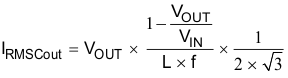
10.2.2.2.2 Output Capacitor Selection
The advanced fast-response voltage mode control scheme of the devices allows the use of tiny ceramic capacitors. Ceramic capacitors with low ESR values have the lowest output voltage ripple and are recommended. The output capacitor requires either an X7R or X5R dielectric. Y5V and Z5U dielectric capacitors, aside from their wide variation in capacitance over temperature, become resistive at high frequencies and can not be used. For most applications, a nominal 10-µF or 22-µF capacitor is suitable. At small ceramic capacitors, the DC-bias effect decreases the effective capacitance. Therefore, a 22-µF capacitor can be used for output voltages higher than 2 V, see the list of capacitors.
In case additional ceramic capacitors in the supplied system are connected to the output of the DC/DC converter, the output capacitor COUT must be decreased to not exceed the recommended effective capacitance range. In this case, a loop stability analysis must be performed as described later.
At nominal load current, the device operates in PWM mode and the RMS ripple current is calculated as: