ZHCSD80B january 2015 – august 2023 TPS62065-Q1 , TPS62067-Q1
PRODUCTION DATA
- 1
- 1 特性
- 2 应用
- 3 说明
- 4 Revision History
- 5 Device Comparison Table
- 6 Pin Configuration and Functions
- 7 Specifications
- 8 Parameter Measurement Information
-
9 Detailed Description
- 9.1 Overview
- 9.2 Functional Block Diagram
- 9.3
Feature Description
- 9.3.1 Mode Selection (TPS62065-Q1) and Forced PWM Mode (TPS62067A-Q1)
- 9.3.2 Power Good (PG, TPS62067x-Q1)
- 9.3.3 Enable
- 9.3.4 Shutdown and Output Discharge
- 9.3.5 Soft Start
- 9.3.6 Undervoltage Lockout (UVLO)
- 9.3.7 Internal Current Limit and Foldback Current Limit For Short-Circuit Protection
- 9.3.8 Clock Dithering
- 9.3.9 Thermal Shutdown
- 9.4 Device Functional Modes
- 10Application and Implementation
- 11Device and Documentation Support
- 12Mechanical, Packaging, and Orderable Information
10.2.2.1 Output Voltage Setting
The output voltage can be calculated to:
Equation 2. 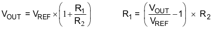
with an internal reference voltage VREF typically 0.6 V.
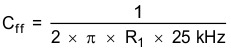
To minimize the current through the feedback divider network, R2 must be within the range of 120 kΩ to 360 kΩ. The sum of R1 and R2 must not exceed approximately 1 MΩ in order to keep the network robust against noise. An external feedforward capacitor, Cff, is required for optimum regulation performance. Lower resistor values can be used. R1 and Cff place a zero in the loop. The right value for Cff can be calculated as:
Equation 3. 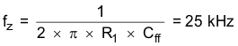
Equation 4.