SLVS294F September 2000 – August 2015 TPS62000 , TPS62002 , TPS62003 , TPS62004 , TPS62005 , TPS62006 , TPS62007 , TPS62008
PRODUCTION DATA.
- 1 Features
- 2 Applications
- 3 Description
- 4 Revision History
- 5 Device Comparison Table
- 6 Pin Configuration and Functions
- 7 Specifications
- 8 Detailed Description
-
9 Application and Implementation
- 9.1 Application Information
- 9.2 Typical Application
- 9.3
System Examples
- 9.3.1 Standard 5-V to 3.3-V/600-mA Conversion; High Efficiency
- 9.3.2 Single Li-ion to 2.5-V/600-mA Using Ceramic Capacitors Only
- 9.3.3 Single Li-ion to 1.8 V/300 mA; Smallest Solution Size
- 9.3.4 Dual Cell NiMH or NiCd to 1.2 V/200 mA; Smallest Solution Size
- 9.3.5 Dynamic Output Voltage Programming As Used in Low Power DSP Applications
- 10Power Supply Recommendations
- 11Layout
- 12Device and Documentation Support
- 13Mechanical, Packaging, and Orderable Information
11 Layout
11.1 Layout Guidelines
As for all switching power supplies, the layout is an important step in the design especially at high peak currents and switching frequencies. If the layout is not carefully done, the regulator might show stability problems as well as EMI problems.
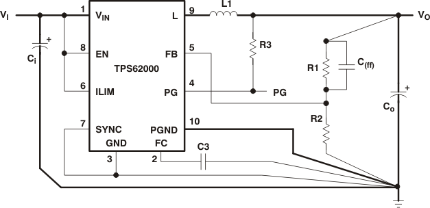
Therefore, use wide and short traces for the main current paths as indicted in bold in Figure 19. The input capacitor should be placed as close as possible to the IC pins as well as the inductor and output capacitor. Place the bypass capacitor, C3, as close as possible to the FC pin. The analog ground, GND, and the power ground, PGND, need to be separated. Use a common ground node as shown in Figure 19 to minimize the effects of ground noise.
11.2 Layout Example
 Figure 19. Layout Diagram