SLVS294F September 2000 – August 2015 TPS62000 , TPS62002 , TPS62003 , TPS62004 , TPS62005 , TPS62006 , TPS62007 , TPS62008
PRODUCTION DATA.
- 1 Features
- 2 Applications
- 3 Description
- 4 Revision History
- 5 Device Comparison Table
- 6 Pin Configuration and Functions
- 7 Specifications
- 8 Detailed Description
-
9 Application and Implementation
- 9.1 Application Information
- 9.2 Typical Application
- 9.3
System Examples
- 9.3.1 Standard 5-V to 3.3-V/600-mA Conversion; High Efficiency
- 9.3.2 Single Li-ion to 2.5-V/600-mA Using Ceramic Capacitors Only
- 9.3.3 Single Li-ion to 1.8 V/300 mA; Smallest Solution Size
- 9.3.4 Dual Cell NiMH or NiCd to 1.2 V/200 mA; Smallest Solution Size
- 9.3.5 Dynamic Output Voltage Programming As Used in Low Power DSP Applications
- 10Power Supply Recommendations
- 11Layout
- 12Device and Documentation Support
- 13Mechanical, Packaging, and Orderable Information
9 Application and Implementation
NOTE
Information in the following applications sections is not part of the TI component specification, and TI does not warrant its accuracy or completeness. TI’s customers are responsible for determining suitability of components for their purposes. Customers should validate and test their design implementation to confirm system functionality.
9.1 Application Information
The TPS6200x device family are highly efficient synchronous step down DC/DC converters providing adjustable output voltages from 0.9 V to VIN and fixed output voltages.
9.2 Typical Application
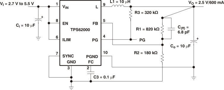 Figure 5. Typical Application Circuit for Adjustable Output Voltage Option
9.2.1 Design Requirements
When the adjustable output voltage version (TPS62000DGS) is used, the output voltage is set by the external resistor divider (see Figure 5).
The output voltage is calculated as:

with R1 + R2 ≤ 1 MΩ
R1 + R2 should not be greater than 1 MW because of stability reasons.
For stability reasons, a small bypass capacitor (C(ff)) is required in parallel to the upper feedback resistor, refer to Figure 5. The bypass capacitor value can be calculated as:


R1 is the upper resistor of the voltage divider. For C(ff), choose a value which comes closest to the computed result.
9.2.2 Detailed Design Procedure
9.2.2.1 Inductor Selection
A 10 μH minimum output inductor is used with the TPS6200x. Values larger than 22 μH or smaller than 10 μH may cause stability problems because of the internal compensation of the regulator.
For output voltages greater than 1.8 V, a 22 μH inductance might be used in order to improve the efficiency of the converter.
After choosing the inductor value of typically 10 μH, two additional inductor parameters should be considered: first the current rating of the inductor and second the DC resistance.
The DC resistance of the inductance influences directly the efficiency of the converter. Therefore, an inductor with lowest DC resistance should be selected for highest efficiency.
In order to avoid saturation of the inductor, the inductor should be rated at least for the maximum output current plus the inductor ripple current which is calculated as:

where
- ƒ = Switching frequency (750 kHz typical)
- L = Inductor value
- ΔIL = Peak-to-peak inductor ripple current
- IL(max) = Maximum inductor current
The highest inductor current occurs at maximum VIN.
A more conservative approach is to select the inductor current rating just for the maximum switch current of the TPS6200x which is 1.6 A with ILIM = VIN and 900 mA with ILIM = GND. See Table 1 for recommended inductors.
Table 1. Tested Inductors
| OUTPUT CURRENT | INDUCTOR VALUE | COMPONENT SUPPLIER | COMMENTS |
|---|---|---|---|
| 0 mA to 600 mA | 10 μH | Coilcraft DO3316P-103 Coilcraft DT3316P-103 Sumida CDR63B-100 Sumida CDRH5D28-100 |
High efficiency |
| Coilcraft DO1608C-103 Sumida CDRH4D28-100 |
Smallest solution | ||
| 0 mA to 300 mA | 10 μH | Coilcraft DO1608C-103 | High efficiency |
| Murata LQH4C100K04 | Smallest solution |
9.2.2.2 Output Capacitor Selection
For best performance, a low ESR output capacitor is needed. At output voltages greater than 1.8 V, ceramic output capacitors can be used to show the best performance. Output voltages below 1.8 V require a larger output capacitor and ESR value to improve the performance and stability of the converter.
Table 2. Capacitor Selection
| OUTPUT VOLTAGE RANGE | OUTPUT CAPACITOR | OUTPUT CAPACITOR ESR |
|---|---|---|
| 1.8 V ≤ VIN ≤ 5.5 V | Co ≥ 10 μF | ESR ≤ 120 mΩ |
| 0.8 V ≤ VIN < 1.8 V | Co ≥ 47 μF | ESR > 50 mΩ |
See Table 3 for recommended capacitors.
If an output capacitor is selected with an ESR value ≤ 120 mΩ, its RMS ripple current rating always meets the application requirements. Just for completeness, the RMS ripple current is calculated as:

The overall output ripple voltage is the sum of the voltage spike caused by the output capacitor ESR plus the voltage ripple caused by charging and discharging the output capacitor:

Where the highest output voltage ripple occurs at the highest input voltage VI.
Table 3. Tested Capacitors
| CAPACITOR VALUE | ESR/mΩ | COMPONENT SUPPLIER | COMMENTS |
|---|---|---|---|
| 10 μF | 50 | Taiyo Yuden JMK316BJ106KL | Ceramic |
| 47 μF | 100 | Sanyo 6TPA47M | POSCAP |
| 68 μF | 100 | Spraque 594D686X0010C2T | Tantalum |
9.2.2.3 Input Capacitor Selection
Because of the nature of the buck converter having a pulsating input current, a low ESR input capacitor is required for best input voltage filtering and minimizing the interference with other circuits caused by high input voltage spikes.
The input capacitor should have a minimum value of 10 μF and can be increased without any limit for better input voltage filtering.
The input capacitor should be rated for the maximum input ripple current calculated as:

The worst case RMS ripple current occurs at D = 0.5 and is calculated as: 
Ceramic capacitor show a good performance because of their low ESR value, and they are less sensitive against voltage transients compared to tantalum capacitors.
Place the input capacitor as close as possible to the input pin of the IC for best performance.
9.2.3 Application Curves
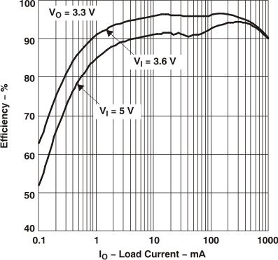 Figure 6. Efficiency vs Load Current
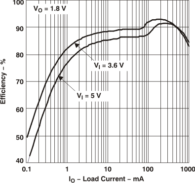 Figure 8. Efficiency vs Load Current
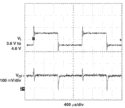 Figure 10. Line Transient Response
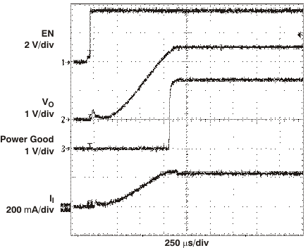 Figure 12. Start-Up vs Time
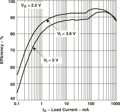 Figure 7. Efficiency vs Load Current
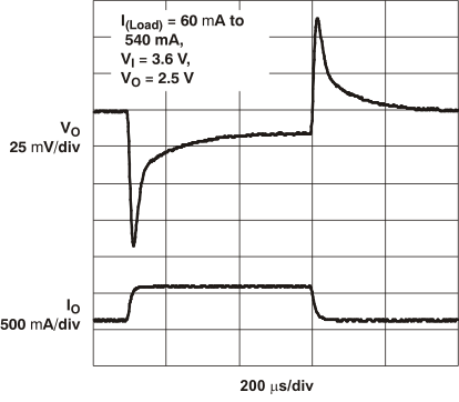 Figure 9. Load Transient Response
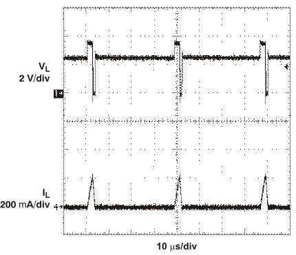 Figure 11. Power Save Mode Operation
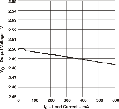 Figure 13. Output Voltage vs Load Current
9.3 System Examples
9.3.1 Standard 5-V to 3.3-V/600-mA Conversion; High Efficiency
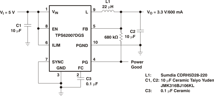 Figure 14. Standard 5-V to 3.3-V/600-mA Conversion; High Efficiency
9.3.2 Single Li-ion to 2.5-V/600-mA Using Ceramic Capacitors Only
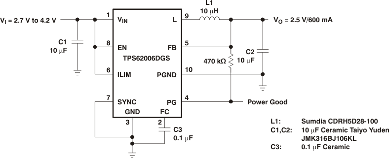 Figure 15. Single Li-ion to 2.5-V/600-mA Using Ceramic Capacitors Only
9.3.3 Single Li-ion to 1.8 V/300 mA; Smallest Solution Size
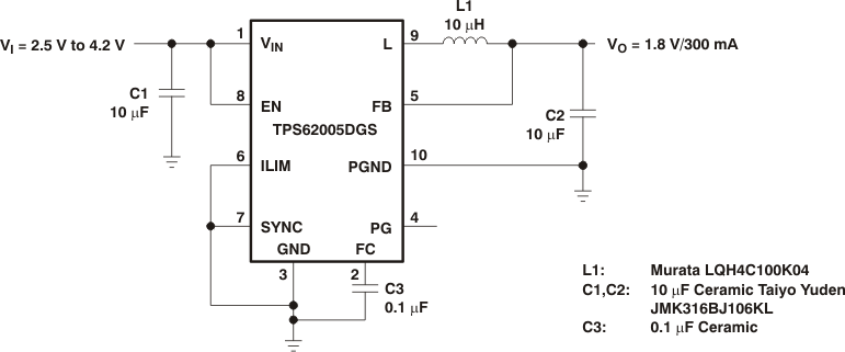
NOTE:
For low noise operation connect SYNC to VIN9.3.4 Dual Cell NiMH or NiCd to 1.2 V/200 mA; Smallest Solution Size
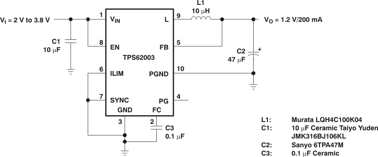 Figure 17. Dual Cell NiMH or NiCd to 1.2 V/200 mA; Smallest Solution Size
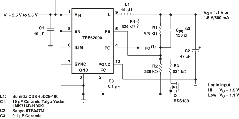
9.3.5 Dynamic Output Voltage Programming As Used in Low Power DSP Applications
