ZHCSG87E February 2017 – August 2019 TPS61178
PRODUCTION DATA.
- 1 特性
- 2 应用
- 3 说明
- 4 修订历史记录
- 5 Device Comparison Table
- 6 Pin Configuration and Functions
- 7 Specifications
-
8 Detailed Description
- 8.1 Overview
- 8.2 Functional Block Diagram
- 8.3
Feature Description
- 8.3.1 Under-voltage Lockout
- 8.3.2 Enable and Disable
- 8.3.3 Startup
- 8.3.4 Load Disconnect Gate Driver
- 8.3.5 Adjustable Peak Current Limit
- 8.3.6 Output Short Protection (with load disconnected FET)
- 8.3.7 Adjustable Switching Frequency
- 8.3.8 External Clock Synchronization (TPS611781)
- 8.3.9 Error Amplifier
- 8.3.10 Slope Compensation
- 8.3.11 Start-up with the Output Pre-Biased
- 8.3.12 Bootstrap Voltage (BST)
- 8.3.13 Over-voltage Protection
- 8.3.14 Thermal Shutdown
- 8.4 Device Functional Modes
-
9 Application and Implementation
- 9.1 Application Information
- 9.2
Typical Application
- 9.2.1 Design Requirements
- 9.2.2 Detailed Design Procedure
- 9.2.3 Setting the Current Limit
- 9.2.4 Setting the Output Voltage
- 9.2.5 TPS61178 Application Waveform
- 9.3 System Examples
- 10Power Supply Recommendations
- 11Layout
- 12器件和文档支持
- 13机械、封装和可订购信息
8.3.5 Adjustable Peak Current Limit
When the TPS61178x is in the normal boost switching phase, the device is prevented from the over current condition via the cycle by cycle current limit by sensing the current through the internal low-side FET. When the peak switch current triggers the current limit threshold, the low-side switch turns off to prevent the switching current further increasing.
The peak switch current limit can be set by a resistor connecting with the ILIMIT pin. The relationship between the current limit and the resistor is determined by Equation 1

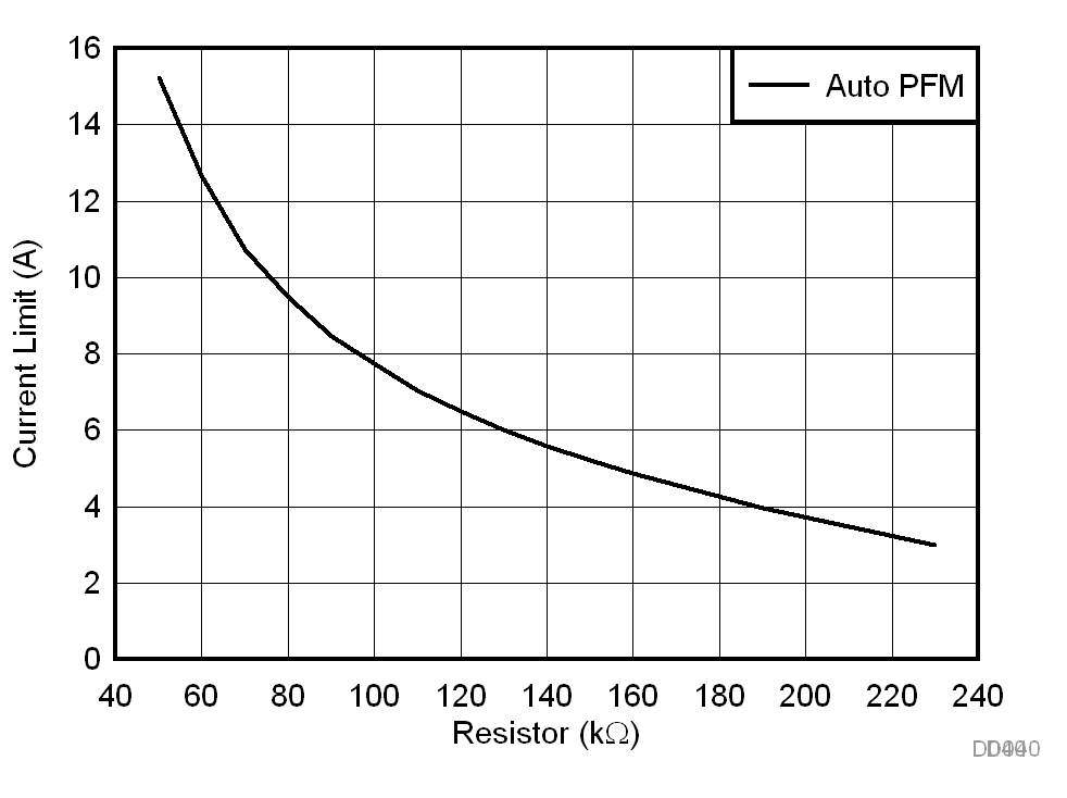
Where RLIMIT is the resistor for setting the current limit, with the unit of kΩ, ILIMIT is switching peak current limit, the unit is A. For instance, when the resistor value is 50 kΩ, the switch peak current limit is 15 A.
Figure 18 shows the current limit versus the setting resistor for both TPS61178 ( Auto PFM ) and TPS611781 ( Forced PWM ) with 7.2-V input to 16-V output.
 Figure 18. Switch Current Limit vs. Setting Resistor
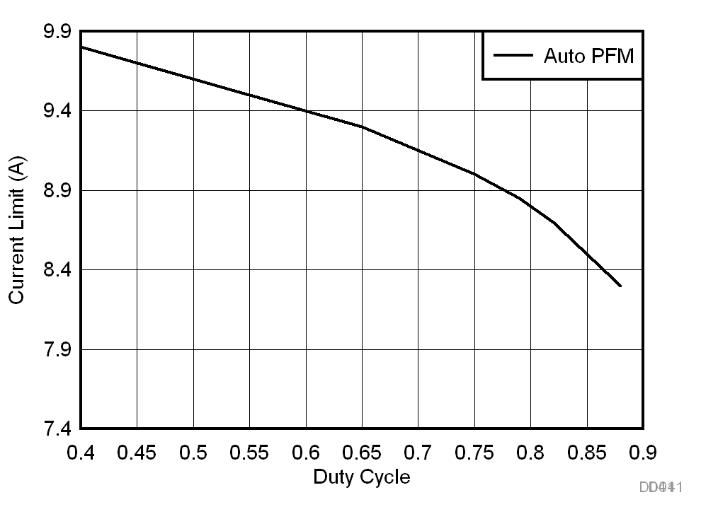
 The current limit value varies with the duty cycle, Figure 30 shows the bench measurement current limit at different duty cycles at RLIMIT = 80.6 kΩ.
 Figure 19. Switch Current Limit vs. Duty Cycle
 For the TPS611781, which works in the Forced PWM mode at the light load, the current limit is typically 0.8 A lower than TPS61178 (Auto PFM) with the same setting resistor.