ZHCSG87E February   2017  – August 2019 TPS61178

PRODUCTION DATA.  

  1. 特性
  2. 应用
  3. 说明
    1.     Device Images
      1.      典型应用
  4. 修订历史记录
  5. Device Comparison Table
  6. Pin Configuration and Functions
    1.     Pin Functions
  7. Specifications
    1. 7.1 Absolute Maximum Ratings
    2. 7.2 ESD Ratings
    3. 7.3 Recommended Operating Conditions
    4. 7.4 Thermal Information
    5. 7.5 Electrical Characteristics
    6. 7.6 Timing Requirements
    7. 7.7 Switching Characteristics
    8. 7.8 Typical Characteristics
  8. Detailed Description
    1. 8.1 Overview
    2. 8.2 Functional Block Diagram
    3. 8.3 Feature Description
      1. 8.3.1  Under-voltage Lockout
      2. 8.3.2  Enable and Disable
      3. 8.3.3  Startup
      4. 8.3.4  Load Disconnect Gate Driver
      5. 8.3.5  Adjustable Peak Current Limit
      6. 8.3.6  Output Short Protection (with load disconnected FET)
      7. 8.3.7  Adjustable Switching Frequency
      8. 8.3.8  External Clock Synchronization (TPS611781)
      9. 8.3.9  Error Amplifier
      10. 8.3.10 Slope Compensation
      11. 8.3.11 Start-up with the Output Pre-Biased
      12. 8.3.12 Bootstrap Voltage (BST)
      13. 8.3.13 Over-voltage Protection
      14. 8.3.14 Thermal Shutdown
    4. 8.4 Device Functional Modes
      1. 8.4.1 Operation
      2. 8.4.2 Auto PFM Mode (TPS61178)
      3. 8.4.3 Forced PWM Mode (TPS611781)
  9. Application and Implementation
    1. 9.1 Application Information
    2. 9.2 Typical Application
      1. 9.2.1 Design Requirements
      2. 9.2.2 Detailed Design Procedure
        1. 9.2.2.1 Custom Design With WEBENCH® Tools
        2. 9.2.2.2 Setting the Switching Frequency
      3. 9.2.3 Setting the Current Limit
      4. 9.2.4 Setting the Output Voltage
        1. 9.2.4.1 Selecting the Inductor
        2. 9.2.4.2 Selecting the Output Capacitors
        3. 9.2.4.3 Selecting the Input Capacitors
        4. 9.2.4.4 Loop Stability and Compensation
          1. 9.2.4.4.1 Small Signal Model
          2. 9.2.4.4.2 Loop Compensation Design Steps
          3. 9.2.4.4.3 Selecting the Disconnect FET
          4. 9.2.4.4.4 Selecting the Bootstrap Capacitor
          5. 9.2.4.4.5 VCC Capacitor
      5. 9.2.5 TPS61178 Application Waveform
    3. 9.3 System Examples
      1. 9.3.1 TPS61178 with 14-V Output from 2.7-V to 4.4-V Input Voltage
      2. 9.3.2 TPS61178 Without Load Disconnect Function
      3. 9.3.3 TPS611781 External Clock Synchronization
  10. 10Power Supply Recommendations
  11. 11Layout
    1. 11.1 Layout Guidelines
    2. 11.2 Layout Example
  12. 12器件和文档支持
    1. 12.1 器件支持
      1. 12.1.1 第三方产品免责声明
      2. 12.1.2 开发支持
        1. 12.1.2.1 使用 WEBENCH® 工具创建定制设计
    2. 12.2 文档支持
      1. 12.2.1 相关文档
    3. 12.3 相关链接
    4. 12.4 接收文档更新通知
    5. 12.5 社区资源
    6. 12.6 商标
    7. 12.7 静电放电警告
    8. 12.8 Glossary
  13. 13机械、封装和可订购信息

封装选项

机械数据 (封装 | 引脚)
散热焊盘机械数据 (封装 | 引脚)
订购信息

Typical Characteristics

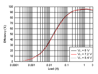
TPS61178 D042_SLVSDA7.gif
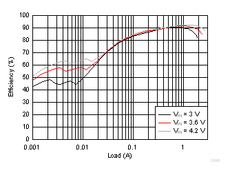
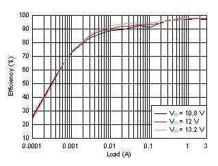
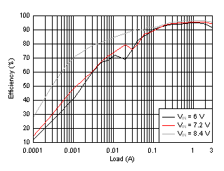
VOUT = 16 V L = 3.3 µH Auto PFM
Figure 1. Efficiency vs. Output Current
TPS61178 D046_SLVSDA7.gif
VOUT = 14 V L = 1.8 µH Auto PFM
Figure 3. Efficiency vs. Output Current
TPS61178 D045_SLVSDA7.gif
VOUT = 16 V L = 3.3 µH Forced PWM
Figure 5. Efficiency vs. Output Current
TPS61178 D048_SLVSDA7.gif
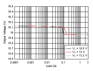
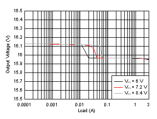
VOUT = 16 V L = 3.3 µH Auto PFM
Figure 7. Output Voltage vs. Load
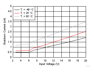
TPS61178 D018_SLVSDA7.gif
Figure 9. Shutdown Current vs VIN
TPS61178 D014_SLVSDA7.gif
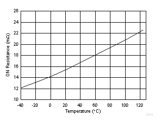
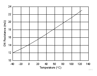
VCC = 6 V
Figure 11. LS Rdson vs Temperature
TPS61178 D032_SLVSDA7.gif
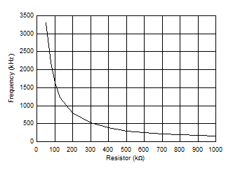
VIN = 7.2 V VOUT = 16 V
Figure 13. Frequency vs Setting Resistor
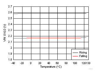
TPS61178 D023_SLVSDA7.gif
Figure 15. VIN UVLO Rising / Falling vs Temperature
TPS61178 D043_SLVSDA7.gif
VOUT = 16 V L = 3.3 µH Auto PFM
Figure 2. Efficiency vs. Output Current
TPS61178 D044_SLVSDA7.gif
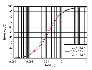
VOUT = 16 V L = 3.3 µH Forced PWM
Figure 4. Efficiency vs. Output Current
TPS61178 D047_SLVSDA7.gif
VOUT = 16 V L = 3.3 µH Auto PFM
Figure 6. Output Voltage vs. Load
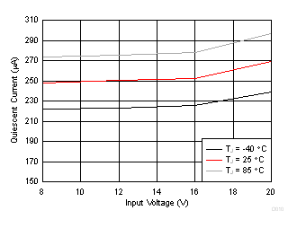
TPS61178 D034_SLVSDA7.gif
Figure 8. Quiescent Current vs VIN
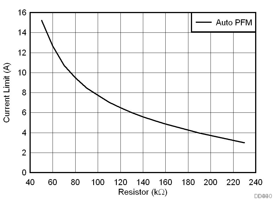
TPS61178 D040_SLVSDA7.gif
VOUT = 16 V VIN = 7.2 V Auto PFM
Figure 10. Switch Current Limit vs Setting Resistor
TPS61178 D013_SLVSDA7.gif
VCC = 6 V
Figure 12. HS Rdson vs Temperature
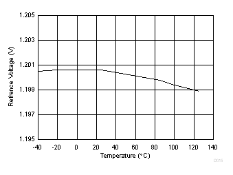
TPS61178 D015_SLVSDA7.gif
Figure 14. Reference Voltage vs Temperature
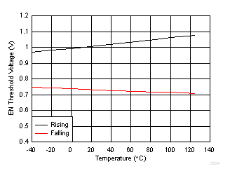
TPS61178 D024_SLVSDA7.gif
Figure 16. EN Threshold Rising / Falling vs Temperature